DNP Achieves 10nm Line Pattern Resolution on Nanoimprint Template for Cutting-Edge Semiconductors
DNP Achieves 10nm Line Pattern Resolution on Nanoimprint Template for Cutting-Edge Semiconductors
- Supports 1.4nm Generation Semiconductors, Reduces Manufacturing Costs and Energy Consumption -
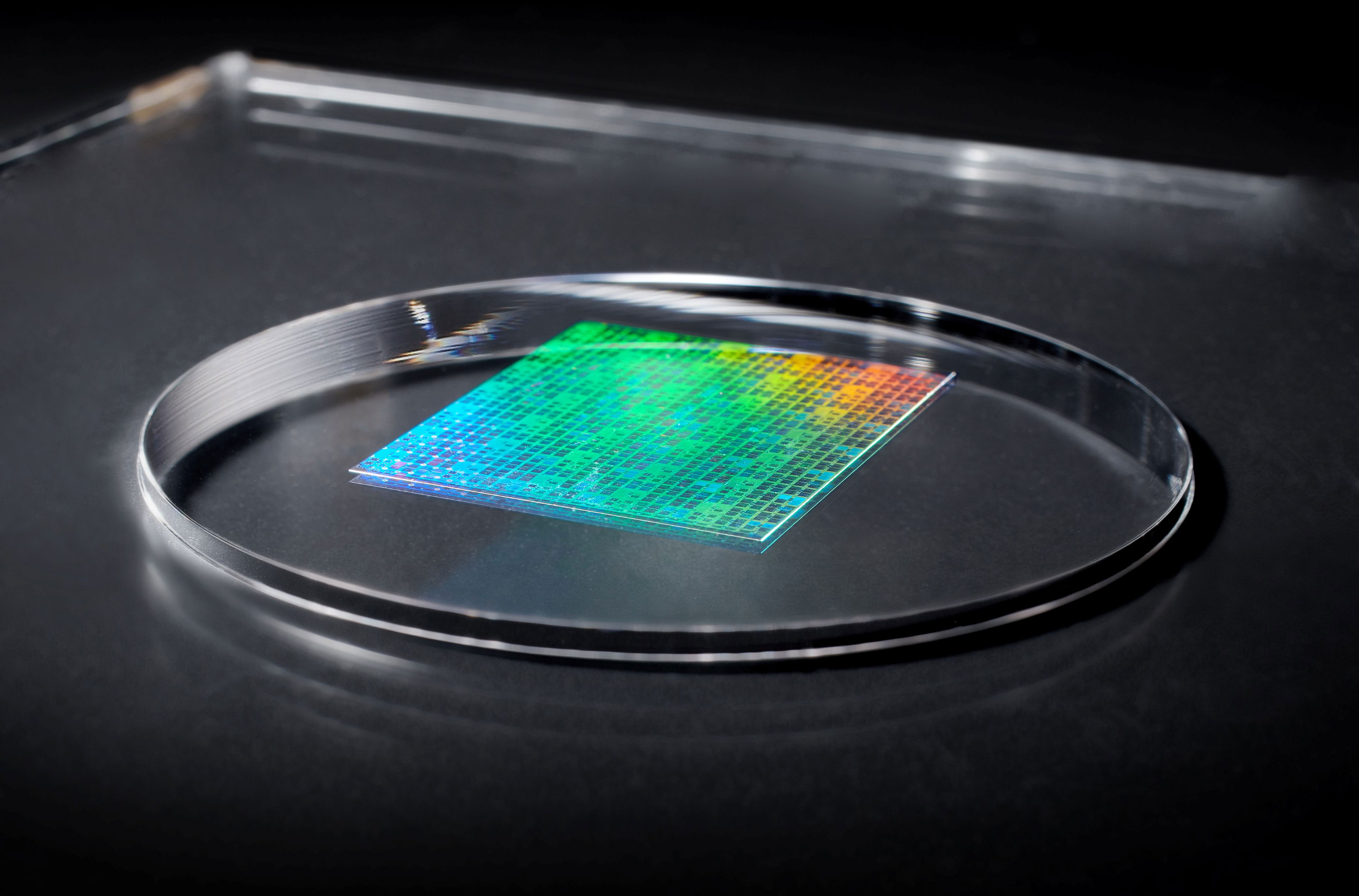
TOKYO--(BUSINESS WIRE)--Dai Nippon Printing Co., Ltd. (DNP, TOKYO:7912) today announced the development of a nanoimprint lithography (NIL) template featuring a circuit line width of 10 nanometers (nm: 10-9 meter). The new template enables patterning for logic semiconductors equivalent to the 1.4nm generation and meets the miniaturization needs of cutting-edge logic semiconductors.
Background and Aims
In line with the shift to more sophisticated devices seen in recent years, demands have emerged for even greater miniaturization in cutting-edge semiconductors, leading to advances in Extreme Ultra-Violet (EUV) lithography-based production. EUV lithography, however, requires substantial capital investment, energy consumption, and operating costs in building production lines and the exposure process.
Since 2003, DNP has been developing NIL templates and has successfully accumulated extensive know-how in high-precision patterning.
In this latest development, DNP has developed a NIL template with a 10nm line pattern. It can replace a portion of the EUV lithography process, facilitating the manufacture of cutting-edge logic semiconductors for clients that do not have EUV lithography production processing.
Key Features
- DNP has successfully achieved the new NIL template with a circuit line width of 10nm by leveraging Self-Aligned Double Patterning (SADP), which doubles pattern density through film deposition and etching a pattern formed by the lithography device.
- The technology also reduces power consumption in the exposure process of cutting-edge semiconductor manufacturing. Driven by an energy-saving processing technology for ultra-fine semiconductors using NIL, it is now possible to reduce power consumption to approximately one-tenth of currently available exposure processes, such as Argon Fluoride (ArF) immersion and EUV.
Going Forward
We have begun evaluation work for NIL templates, and aim to start mass production in 2027. DNP will advance the further development of NIL templates and enhance production capacity to meet growing demand, targeting increased NIL sales of 4 billion yen in FY 2030.
DNP was established in 1876, and has become a leading global company that leverages print-based solutions to engineer fresh business opportunities while protecting the environment and creating a more vibrant world for all. We capitalize on core competencies in microfabrication and precision coating technology to provide products for the display, electronic devices, and optical film markets.
Contacts
Media contact
DNP: Yusuke Kitagawa, +81-3-6735-0101
kitagawa-y3@mail.dnp.co.jp