Avicena Names Marco Chisari as New CEO
Avicena Names Marco Chisari as New CEO
Amid unprecedented demand for ultra-low power optical interconnects in AI datacenters and future disaggregated memory fabrics, Avicena is poised for the next phase of growth
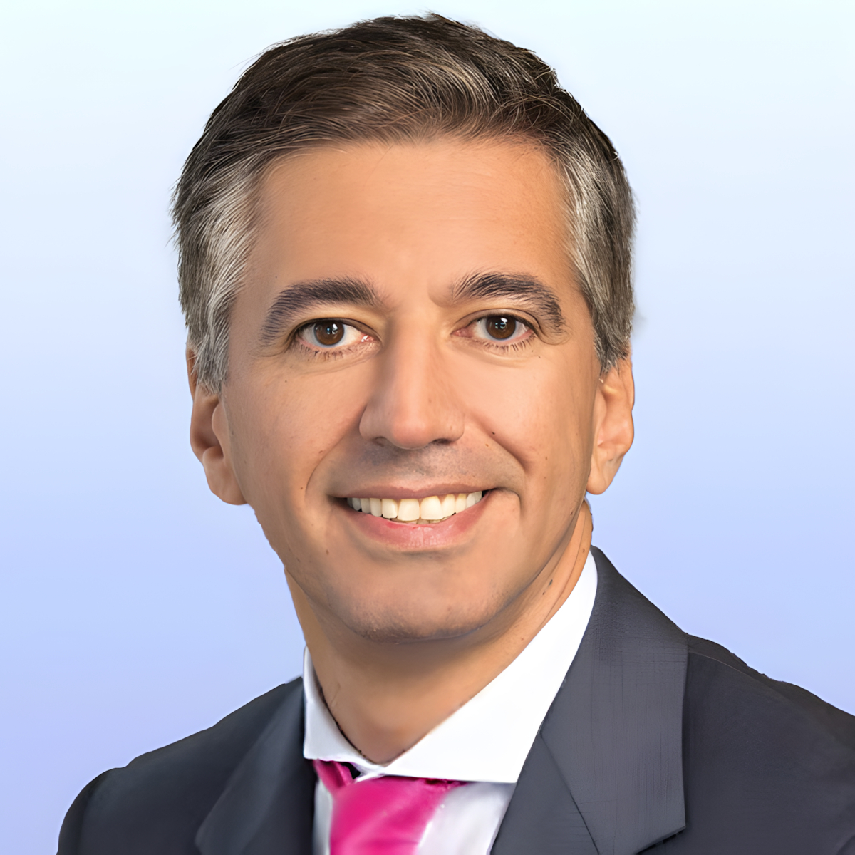
SUNNYVALE, Calif.--(BUSINESS WIRE)--Avicena, the leader in ultra-low power high-density microLED-based interconnects, announced today that Marco Chisari, former Executive Vice President, Head of Samsung Foundries and Head of the Samsung Semiconductor Innovation Center (SSIC), has joined Avicena as the Chief Executive Officer (CEO) and a member of the board of directors (Board). Marco succeeds co-founder and CEO Bardia Pezeshki, who will assume the role of Chief Technology Officer (CTO).
“I am very impressed by Avicena’s technology, patent portfolio, ecosystem and customer traction. The goal is to realize the full potential of the technology and bring it into the AI market.”
Share
“We are thrilled to welcome Marco to Avicena as we enter our next stage of growth,” said Bardia Pezeshki. “With his career in the semiconductor industry, corporate development and investment banking, he is well positioned to lead Avicena to growth in the rapidly evolving AI datacenter interconnect market.” The company has recently raised $65 million in Series B Funding led by Tiger Global with the participation from several new and existing investors.
“Artificial intelligence (AI) is driving an unprecedented surge in demand for compute and memory performance. Avicena’s groundbreaking LightBundleTM technology, based on high-speed microLED, is uniquely positioned to deliver the ultra-low power high-capacity interconnects that the industry needs,” said Marco Chisari. “I am very impressed by Avicena’s technology, patent portfolio, ecosystem and customer traction. The goal is to realize the full potential of the technology and bring it into the AI market.”
Marco Chisari has over 25 years of experience with global Fortune 500 organizations, such as Nokia, STMicroelectronics, SAMSUNG, Mubadala, GlobalFoundries, JPMorgan, Credit Suisse and Bank of America Merrill Lynch, both in the semiconductor industry and in the financial and investment banking sectors. Marco moved to Silicon Valley as a microelectronic engineer designing flash memories at STMicroelectronics. He transitioned to investment banking at JPMorgan in London, working on major technology M&A and IPOs. At Mubadala, he led investments and acquisitions that contributed to the creation of GlobalFoundries, including the acquisition of IBM Microelectronics. Later, as Global Head of Semiconductor Investment Banking at Bank of America Merrill Lynch, he managed some of the largest recent M&A deals in the semiconductor industry. Most recently, he served as Executive Vice President at Samsung Electronics running the U.S. foundry business and the Samsung Innovation Center in the U.S.
About Avicena
Avicena is a privately held company located in Sunnyvale, CA, with a subsidiary in Edinburgh, Scotland. The company was founded in 2019 by leading technologists from the optical networking industry with a track record of delivering breakthrough products. Avicena is the first company to use microLEDs for high-speed communications. Unlike laser-based alternatives, Avicena’s µLED interconnects enable GPU clusters to Scale Up across multiple racks, connecting thousands of GPUs, while delivering industry-leading sub-pJ/bit energy efficiency. These interconnects unlock scalable, energy-efficient performance far beyond the limit of copper. This technology is a key building block in the evolution of networking and computing that will reduce the energy impact on our planet.
For more information, visit https://avicena.tech.
Contacts
Avicena Media Contact:
Sama Pourmojib
email: sama@avicena.tech