Cadence Accelerates Development of Billion-Gate AI Designs with Innovative Power Analysis Technology Built on NVIDIA
Cadence Accelerates Development of Billion-Gate AI Designs with Innovative Power Analysis Technology Built on NVIDIA
New Cadence Palladium Dynamic Power Analysis App enables designers of AI/ML chips and systems to create more energy-efficient designs and accelerate time to market
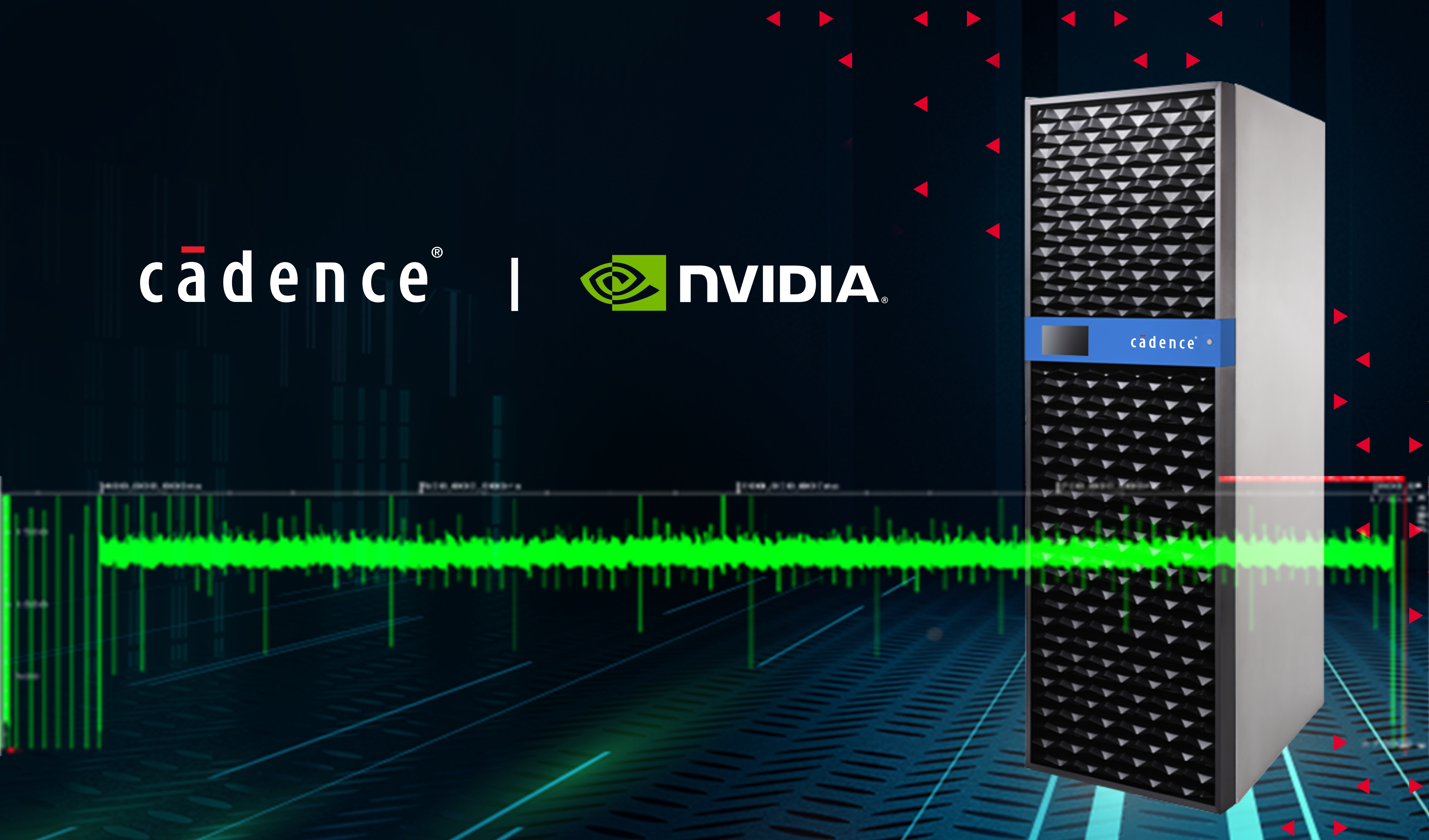
SAN JOSE, Calif.--(BUSINESS WIRE)--Cadence (Nasdaq: CDNS) today announced a significant leap forward in the power analysis of pre-silicon designs through its close collaboration with NVIDIA. Leveraging the advanced capabilities of the Cadence® Palladium® Z3 Enterprise Emulation Platform, utilizing the new Cadence Dynamic Power Analysis (DPA) App, Cadence and NVIDIA have achieved what was previously considered impossible: hardware accelerated dynamic power analysis of billion-gate AI designs, spanning billions of cycles within a few hours with up to 97 percent accuracy. This milestone enables semiconductor and systems developers targeting AI, machine learning (ML) and GPU-accelerated applications to design more energy-efficient systems and accelerate their time to market.
This project redefined boundaries, processing billions of cycles in as few as two to three hours. This empowers customers to confidently meet aggressive performance and power targets and accelerate their time to silicon.
Share
The massive complexity and computational requirements of today’s most advanced semiconductors and systems present a challenge for designers, who have until now been unable to accurately predict their power consumption under realistic conditions. Conventional power analysis tools cannot scale beyond a few hundred thousand cycles without requiring impractical timelines. In close collaboration with NVIDIA, Cadence has overcome these challenges through hardware-assisted power acceleration and parallel processing innovations, enabling previously unattainable precision across billions of cycles in early-stage designs.
“Cadence and NVIDIA are building on our long history of introducing transformative technologies developed through deep collaboration,” said Dhiraj Goswami, corporate vice president and general manager at Cadence. “This project redefined boundaries, processing billions of cycles in as few as two to three hours. This empowers customers to confidently meet aggressive performance and power targets and accelerate their time to silicon.”
"As the era of agentic AI and next-generation AI infrastructure rapidly evolves, engineers need sophisticated tools to design more energy-efficient solutions," said Narendra Konda, vice president, Hardware Engineering at NVIDIA. “By combining NVIDIA’s accelerated computing expertise with Cadence’s EDA leadership, we’re advancing hardware-accelerated power profiling to enable more precise efficiency in accelerated computing platforms.”
The Palladium Z3 Platform uses the DPA App to accurately estimate power consumption under real-world workloads, allowing functionality, power usage and performance to be verified before tapeout, when the design can still be optimized. Especially useful in AI, ML and GPU-accelerated applications, early power modeling increases energy efficiency while avoiding delays from over- or under-designed semiconductors. Palladium DPA is integrated into the Cadence analysis and implementation solution to allow designers to address power estimation, reduction and signoff throughout the entire design process, resulting in the most efficient silicon and system designs possible.
For more information, please visit the Cadence Palladium web page.
About Cadence
Cadence is a market leader in AI and digital twins, pioneering the application of computational software to accelerate innovation in the engineering design of silicon to systems. Our design solutions, based on Cadence’s Intelligent System Design™ strategy, are essential for the world’s leading semiconductor and systems companies to build their next-generation products from chips to full electromechanical systems that serve a wide range of markets, including hyperscale computing, mobile communications, automotive, aerospace, industrial, life sciences and robotics. In 2024, Cadence was recognized by the Wall Street Journal as one of the world’s top 100 best-managed companies. Cadence solutions offer limitless opportunities—learn more at www.cadence.com.
© 2025 Cadence Design Systems, Inc. All rights reserved worldwide. Cadence, the Cadence logo and the other Cadence marks found at www.cadence.com/go/trademarks are trademarks or registered trademarks of Cadence Design Systems, Inc. All other trademarks are the property of their respective owners.
Category: Featured
Contacts
For more information, please contact:
Cadence Newsroom
408-944-7039
newsroom@cadence.com