KYOCERA to Construct New R&D Center in Kirishima City, Kagoshima, Japan
KYOCERA to Construct New R&D Center in Kirishima City, Kagoshima, Japan
New facility at Kyocera Kokubu Campus will expand R&D speed, capabilities
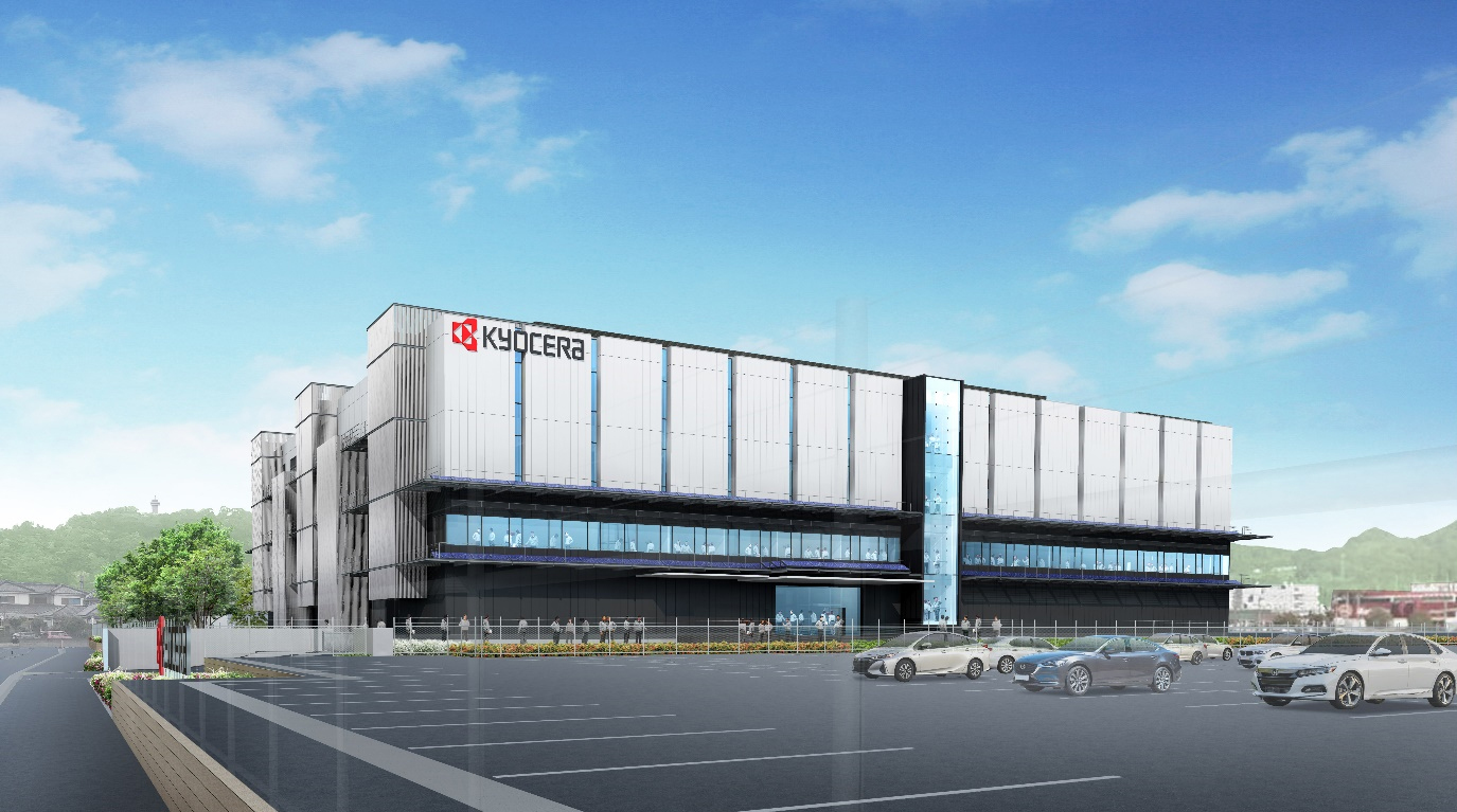
KYOTO, Japan--(BUSINESS WIRE)--Kyocera Corporation (President: Hideo Tanimoto, hereafter “Kyocera”) today announced it will begin construction of a new research and development center in January 2021 at its Kokubu campus in Kirishima City, Kagoshima, Japan. Kyocera has executed a location agreement with the mayor of Kirishima City for the new R&D center, which will focus on new innovations in the fields of information and communications, environmental preservation, and smart energy.
The Kokubu campus is already an innovation hub and site of three strategic R&D groups: Kyocera’s Monozukuri R&D Laboratory, which focuses on advanced material technologies; its Production Technology Division, focusing on manufacturing process innovation; and its Analysis Center, which develops simulation and evaluation technologies. R&D programs at the campus currently include 5G smartphone technologies, electronic and semiconductor components used in IoT devices, and key components for new smart energy technologies, such as cell stacks for Solid Oxide Fuel Cells (SOFCs). Intellectual property developed there has found a wide range of other applications as well, in the automotive, aerospace, medical and healthcare fields.
Through greater collaboration among these R&D operations, Kyocera will establish a new platform to accelerate development and production efforts, with comprehensive support for manufacturing new products, promoting factory automation, and improving manufacturing efficiencies. Kyocera will position the new facility specifically as an incubator for open innovation, sharing technical information for human resource development, and networking with inventors outside of Kyocera.
Outline of Kyocera’s New R&D Center
Name |
(To be announced) |
Location |
Kyocera’s Kagoshima Kokubu Plant Campus 1450-1 Azadainomaru, Kokubukamikogawa, Kirishima-shi, Kagoshima Prefecture, Japan |
Total investment |
Approximately 10 billion yen (approx. 96 million U.S. dollars) |
Building area |
5,990 m2 steel construction with 5 stories |
Total floor space |
22,902 m2 |
Construction plan |
Construction begins: January 2021 Facility opens: September 2022 |
Main R&D activities |
Development of laminated ceramic capacitors, ceramic packages for electronic devices, cell stacks for SOFCs |
Kyocera Corporation (TOKYO:6971, https://global.kyocera.com/), the parent and global headquarters of the Kyocera Group, was founded in 1959 as a producer of fine ceramics (also known as “advanced ceramics”). By combining these engineered materials with metals and integrating them with other technologies, Kyocera has become a leading supplier of industrial and automotive components, semiconductor packages, electronic devices, smart energy systems, printers, copiers, and mobile phones. During the year ended March 31, 2020, the company’s consolidated sales revenue totaled 1.6 trillion yen (approx. US$14.7 billion). Kyocera is ranked #549 on Forbes magazine’s 2020 “Global 2000” list of the world’s largest publicly traded companies.
Contacts
KYOCERA Corporation (Japan), Corporate Communications
Kenichi Hara, Tel: +81-(0)75-604-3416
Fax: +81-(0)75-604-3516
webmaster.pressgl@kyocera.jp