Cadence Accelerates SoC, 3D-IC and Chiplet Design for AI Data Centers, Automotive and Connectivity in Collaboration with Samsung Foundry
Cadence Accelerates SoC, 3D-IC and Chiplet Design for AI Data Centers, Automotive and Connectivity in Collaboration with Samsung Foundry
Expanded collaboration includes new multi-year IP agreement and joint development of advanced AI-driven flows on latest SF2P process node
SAN JOSE, Calif.--(BUSINESS WIRE)--Cadence (Nasdaq: CDNS) today announced an expansion of its collaboration with Samsung Foundry, including a new multi-year IP agreement to broaden Cadence® memory and interface IP solutions in Samsung Foundry’s SF4X, SF5A and SF2P advanced process nodes. Furthering their ongoing technology collaboration, the companies are leveraging Cadence’s AI-driven design solutions and Samsung’s advanced SF4X, SF4U and SF2P process nodes to deliver high-performance, low-power solutions for AI data center, automotive—including advanced driver-assistance systems (ADAS)—and next-generation RF connectivity applications.
Cadence’s AI-driven design solutions and comprehensive portfolio of IP and silicon solutions enhance designers’ productivity and accelerate time to market (TTM) for leading-edge SoCs, chiplets and 3D-ICs on advanced Samsung Foundry processes.
Share
Cadence’s AI-driven design solutions and comprehensive portfolio of IP and silicon solutions enhance designers’ productivity and accelerate time to market (TTM) for leading-edge SoCs, chiplets and 3D-ICs on advanced Samsung Foundry processes.
“We support a full portfolio of IP, subsystems and chiplets on the Samsung Foundry process nodes, and our latest multi-year IP agreement strengthens our ongoing collaboration,” said Boyd Phelps, senior vice president and general manager of the Silicon Solutions Group at Cadence. “By combining Cadence’s AI-driven design and silicon solutions with Samsung’s advanced processes, we’re delivering the leading-edge technologies our mutual customers need to innovate and bring their products to market faster.”
Hyung-Ock Kim, vice president and head of the Foundry Design Technology Team at Samsung Electronics, added, “Cadence’s suite of digital tools from RTL to GDS is now certified for Samsung’s latest SF2P process node, supporting advancements like Hyper Cell and LLE 2.0 technologies. Cadence and Samsung are also collaborating closely to enable analog migration, enhance power integrity and improve thermal and warpage analyses for 3D-ICs using GPU acceleration. Additionally, a multi-year agreement between Cadence and Samsung Foundry to expand memory and interface IP solutions further strengthens our partnership.”
Expanded IP Agreement
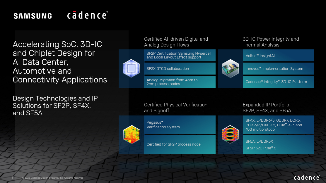
Cadence and Samsung Foundry signed a new multi-year agreement to deliver advanced memory and interface IP solutions targeting AI, high-performance computing (HPC) and automotive applications. The expanded SF4X IP portfolio includes LPDDR6/5x-14.4G, GDDR7-36G, DDR5-9600, PCI Express® (PCIe®) 6.0/5.0/CXL 3.2, Universal Chiplet Interconnect Express™ (UCIe™)-SP 32G and 10G multi-protocol PHY (USB3.x, DP-TX, PCIe 3.0 and SGMII) with companion controller IP, enabling a complete subsystem silicon solution. LPDDR5X-8533 PHY IP tailored for automotive applications rounds out the SF5A IP platform solution, and the addition of a new 32G PCIe 5.0 PHY to the existing SF2P offering serves leading AI/HPC customers’ needs.
Digital Full Flow Certification and Advanced Digital Technology Developments
Based on an extensive design and technology co-optimization (DTCO) project, the Cadence digital full flow has been certified for the latest Samsung SF2P process node, including the Samsung Hyper Cell methodology. In addition, Cadence implemented support for Samsung Local Layout Effect (LLE) timing accuracy. Cadence and Samsung are also collaborating on DTCO for next-generation process nodes.
The Cadence Pegasus™ Verification System is certified for Samsung SF2P and additional Samsung nodes. The Cadence physical verification flow is optimized to allow mutual customers to achieve signoff accuracy and runtime goals using massive scalability, enabling faster TTM.
Analog Design Migration
Cadence and Samsung Foundry have successfully automated the migration of analog cell-based 4nm IP to the advanced 2nm process node, enabling faster turnaround time while maintaining functional and design intent. This migration highlights the importance of technology scaling and IP reuse to save time and development costs and sets the stage for future migrations of analog cells and other IP across various process nodes.
RF Chip/Package Co-Design Reference Flow Collaboration
Cadence and Samsung Foundry also successfully demonstrated a comprehensive Front-End Module (FEM)/Antenna-in-Package (AiP) co-design flow for next-generation mmWave applications based on Samsung’s 14nm FinFET process. Design turnaround time was accelerated by streamlining design data management between each stage of IC/module development from initial system-level budgeting through RFIC/package co-design, analysis and post-layout verification.
Power Integrity for 3D-IC
Cadence and Samsung collaborated on comprehensive full-flow power integrity analysis for 3D-ICs spanning the entire process, from early exploration to final signoff, and employing advanced Cadence EDA tools, including Voltus™ InsightAI, the Innovus™ Implementation System and the Integrity™ 3D-IC Platform. Applied to a high-speed CPU chip using Samsung’s SF2 node, Voltus InsightAI achieved an impressive 80-90% resolution of IR-drop violations with minimal timing and power impact, showcasing its ability to balance power integrity with performance needs.
About Cadence
Cadence is a market leader in AI and digital twins, pioneering the application of computational software to accelerate innovation in the engineering design of silicon to systems. Our design solutions, based on Cadence’s Intelligent System Design™ strategy, are essential for the world’s leading semiconductor and systems companies to build their next-generation products from chips to full electromechanical systems that serve a wide range of markets, including hyperscale computing, mobile communications, automotive, aerospace, industrial, life sciences and robotics. In 2024, Cadence was recognized by the Wall Street Journal as one of the world’s top 100 best-managed companies. Cadence solutions offer limitless opportunities—learn more at www.cadence.com.
© 2025 Cadence Design Systems, Inc. All rights reserved worldwide. Cadence, the Cadence logo and the other Cadence marks found at www.cadence.com/go/trademarks are trademarks or registered trademarks of Cadence Design Systems, Inc. PCI Express and PCIe are registered trademarks of PCI-SIG. Universal Chiplet Interconnect Express and UCIe are trademarks of the UCIe Consortium. All other trademarks are the property of their respective owners.
Category: Featured
Contacts
For more information, please contact:
Cadence Newsroom
408-944-7039
newsroom@cadence.com