

Alphawave Semi Expands Partnership with Samsung Foundry to Further Drive Innovation at Advanced Semiconductor Nodes
Alphawave Semi Expands Partnership with Samsung Foundry to Further Drive Innovation at Advanced Semiconductor Nodes
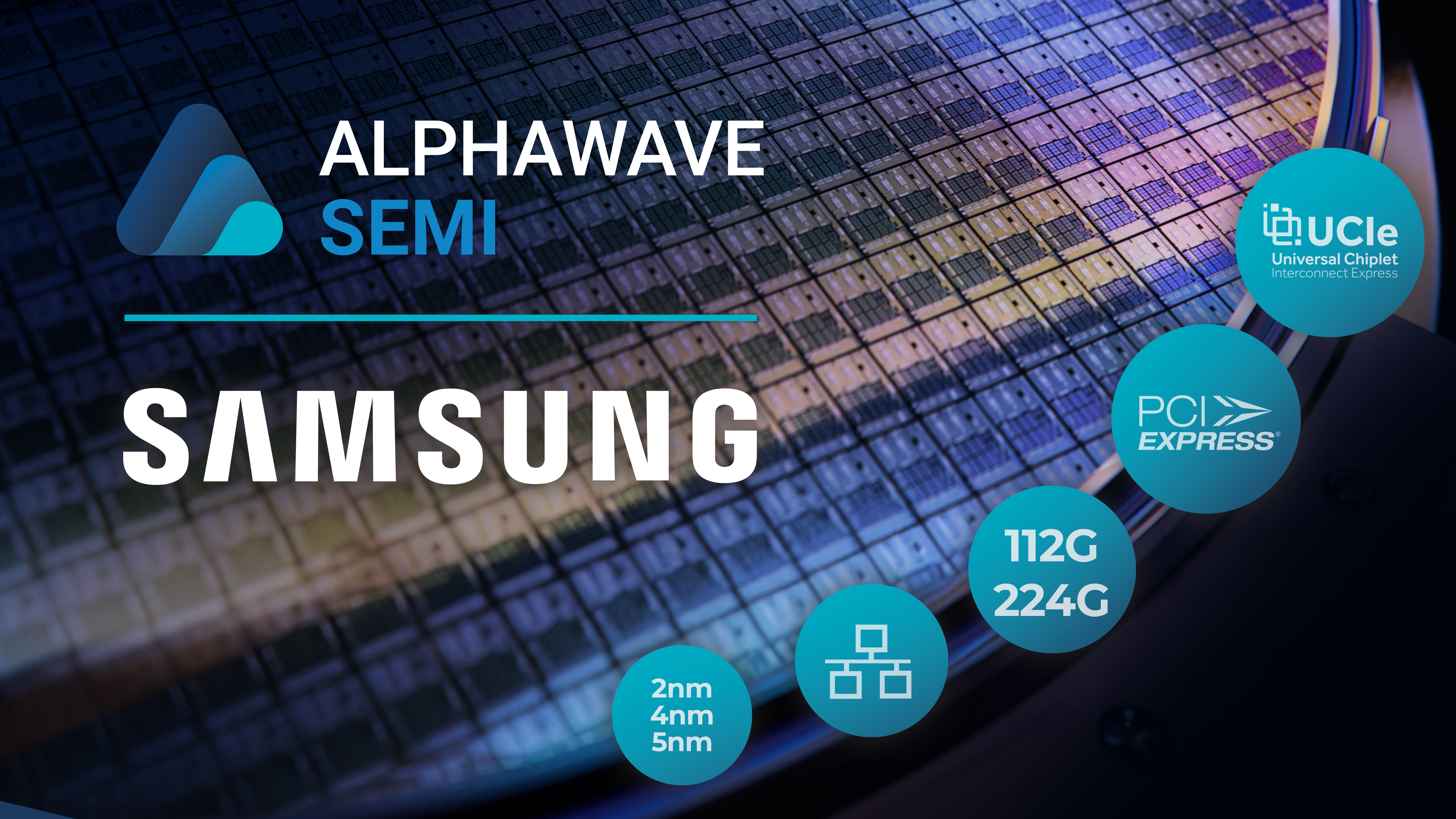
Extensive range of IP for processes down to 2nm encompasses leading-edge technology for PCIe 7.0, 112G and 224G Ethernet, and UCIe
LONDON & TORONTO--(BUSINESS WIRE)--Alphawave Semi (LSE: AWE), a global leader in high-speed connectivity and compute silicon for the world’s technology infrastructure, has announced the expansion of its strategic partnership with Samsung Foundry, one of the world's leading advanced semiconductor manufacturers.
The expanded agreement encompasses leading-edge IP for PCI Express 7.0, 112G and 224G Ethernet and the latest UCIe (Universal Chiplet Interconnect Express) die-to-die interconnect standard that is enabling next-generation SoC (system-on-chip) technologies for AI and other HPC systems.
Alphawave Semi’s partnership with Samsung Foundry is based on an extensive range of IP aimed at minimizing design risks and propelling the success of high-performance silicon and next-generation chiplets for sectors such as artificial intelligence (AI), high-performance computing (HPC), data networking, autonomous vehicles and solid-state storage (SSD). The latest expansion of the collaboration expands these offerings for Samsung’s cutting-edge SF5 (5nm), SF4 (4nm), and SF2 (2nm) processes with additional, state-of-the-art IP that is essential for next-generation compute and network connectivity.
"Strengthening our collaboration with Samsung Foundry marks a significant step forward in our mission to drive the future of high-speed connectivity," said Alphawave Semi CTO Tony Chan Carusone. "This partnership leverages both Alphawave Semi’s leading-edge IP portfolio and Samsung’s manufacturing prowess to meet the fast-growing demands of high-performance computing and networking."
"We are excited to strengthen our partnership with Alphawave Semi," said Jongshin Shin, Corporate EVP of foundry IP development at Samsung Foundry. "By harnessing their cutting-edge IP technologies alongside our advanced semiconductor processes, this collaboration is set to redefine benchmarks for high-speed connectivity and high-performance computing, supporting the ongoing evolution and success of next-generation AI systems and network solutions."
For more information about Alphawave Semi and our partnership with Samsung Foundry, please visit www.awavesemi.com
About Alphawave Semi
Alphawave Semi is a global leader in high-speed connectivity and compute silicon for the world’s technology infrastructure. Faced with the exponential growth of data, Alphawave Semi’s technology services a critical need: enabling data to travel faster, more reliably, and with higher performance at lower power. We are a vertically integrated semiconductor company, and our IP, custom silicon, and connectivity products are deployed by global tier-one customers in data centers, compute, networking, AI, 5G, autonomous vehicles, and storage. Founded in 2017 by an expert technical team with a proven track record in licensing semiconductor IP, our mission is to accelerate the critical data infrastructure at the heart of our digital world. To find out more about Alphawave Semi, visit: awavesemi.com.
Alphawave Semi and the Alphawave Semi logo are trademarks of Alphawave IP Group plc. All rights reserved.
Contacts
Claudia Cano-Manuel
Grand Bridges Marketing Limited
press@awavesemi.com
+44 7562 182327