Samsung Electronics Begins Industry's First Mass Production of 9th-Gen V-NAND
Samsung Electronics Begins Industry's First Mass Production of 9th-Gen V-NAND
Industry-leading bit density with about 50% increase compared to previous generation
Productivity for the V-NAND’s groundbreaking double-stack structure enhanced through advanced ‘channel hole etching’ technology
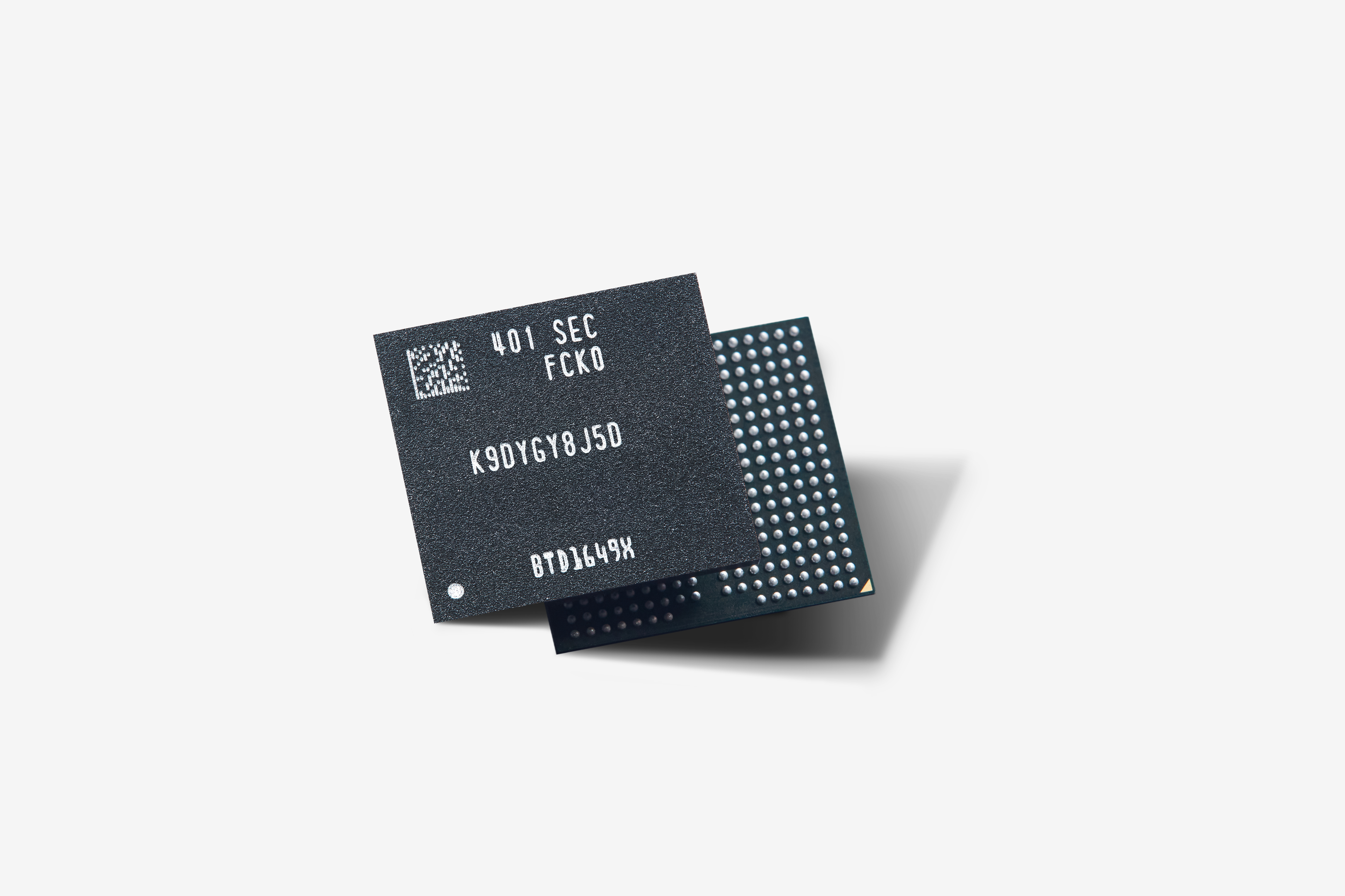
SEOUL, South Korea--(BUSINESS WIRE)--Samsung Electronics Co., Ltd., the world leader in advanced memory technology, today announced that it has begun mass production for its one-terabit (Tb) triple-level cell (TLC) 9th-generation vertical NAND (V-NAND), solidifying its leadership in the NAND flash market.
“We are excited to deliver the industry’s first 9th-gen V-NAND, which will bring future applications leaps forward. In order to address the evolving needs for NAND flash solutions, Samsung has pushed the boundaries in cell architecture and operational scheme for our next-generation product,” said SungHoi Hur, Head of Flash Product & Technology of the Memory Business at Samsung Electronics. “Through our latest V-NAND, Samsung will continue to set the trend for the high-performance, high-density solid state drive (SSD) market that meets the needs for the coming AI generation.”
With the industry's smallest cell size and thinnest mold, Samsung improved the bit density of the 9th-generation V-NAND by about 50% compared to the 8th-generation V-NAND. New innovations such as cell interference avoidance and cell life extension have been applied to enhance product quality and reliability, while eliminating dummy channel holes has significantly reduced the planar area of the memory cells.
In addition, Samsung’s advanced "channel hole etching" technology showcases the company’s leadership in process capabilities. This technology creates electron pathways by stacking mold layers and maximizes fabrication productivity as it enables simultaneous drilling of the industry's highest cell layer count in a double-stack structure. As the number of cell layers increase, the ability to pierce through higher cell numbers becomes essential, demanding more sophisticated etching techniques.
The 9th-generation V-NAND is equipped with the next-generation NAND flash interface, "Toggle 5.1," which supports increased data input/output speeds by 33% to up to 3.2 gigabits-per-second (Gbps). Along with this new interface, Samsung plans to solidify its position within the high-performance SSD market by expanding support for PCIe 5.0.
Power consumption has also been improved by 10% with advancements in low-power design, compared to the previous generation. As reducing energy usage and carbon emissions become vital for customers, Samsung's 9th-generation V-NAND is expected to be an optimal solution for future applications.
Samsung has started mass production for the 1Tb TLC 9th-generation V-NAND this month, followed by the quad level cell (QLC) model in the second half of this year.
About Samsung Electronics Co., Ltd.
Samsung inspires the world and shapes the future with transformative ideas and technologies. The company is redefining the worlds of TVs, smartphones, wearable devices, tablets, home appliances, network systems, and memory, system LSI, foundry and LED solutions, and delivering a seamless connected experience through its SmartThings ecosystem and open collaboration with partners. For the latest news, please visit the Samsung Newsroom at news.samsung.com.
Contacts
Ujeong Jahnke
Samsung Semiconductor Europe GmbH
Tel. +49(0)89-45578-1000
Email: sseg.comm@samsung.com