Avicena Announces Scalable Sub-pJ/bit LightBundle™ Chiplet Interconnect with 10m Reach
Avicena Announces Scalable Sub-pJ/bit LightBundle™ Chiplet Interconnect with 10m Reach
Avicena is unveiling a modular interconnect platform with multi-Tbps/mm shoreline density based on its LightBundle™ microLED technology, supporting a wide range of die-to-die interfaces.
SAN DIEGO--(BUSINESS WIRE)--Avicena, headquartered in Sunnyvale, CA, is announcing its new scalable LightBundle chiplet interconnect at OFC 2024 in San Diego, CA (https://www.ofcconference.org/en-us/home/). The chiplet interconnect extends ultra-high density die-to-die (D2D) connections up to 10m at multi-Tbps/mm shoreline bandwidth density and class leading sub-pJ/bit energy efficiency. Based on Avicena’s LightBundle platform which supports unprecedented shoreline density and energy efficiency, it unlocks increased performance from HPC and AI cluster architectures.
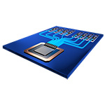
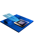
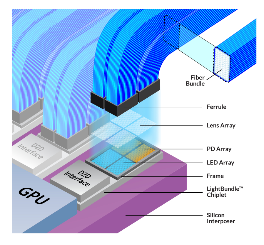
Scalable LightBundle Chiplet Platform for D2D Interconnects
Artificial intelligence (AI) is driving an unprecedented surge in demand for compute and memory performance, driven by applications like ChatGPT based on large language models (LLMs). This requires ever higher density, lower power, longer interconnects between processors and different types of memory modules.
Today, High Bandwidth Memory (HBM) modules must be located within a few millimeters of a Graphics Processing Unit (GPU), limiting accessible memory bandwidth and capacity based on GPU shoreline. The LightBundle chiplet interconnect extends HBM and other ultra-high performance D2D connections up to 10m while dissipating < 1pJ/bit for the optical interconnect and supporting multi-Tbps/mm beachfront density. This enables GPUs and other high-performance ICs to greatly increase their total IO bandwidth, accessing vastly more HBM and relieving inter-processor bottlenecks. The LightBundle chiplet is compatible with standard multichip packaging and supports a wide range of D2D interfaces including standard and advanced versions of UCIe and BOW. Avicena is working with selected partners on different implementations. Initial prototypes will be available in the second half of 2025.
“At Avicena, we are excited to announce our ultra-low power scalable chiplet interconnect based on our LightBundle platform,” says Bardia Pezeshki, Founder and CEO of Avicena. “The first D2D implementation will be an 8Tbps UCIe advanced interconnect with a total chiplet footprint of 4mm x 7mm, beachfront density of 2Tbps/mm and power consumption of < 12W.”
“As generative AI continues to evolve, the role of high bandwidth-density, low-power and low latency interconnects between GPUs and HBM modules cannot be overstated”, says Vlad Kozlov, Founder & CEO of LightCounting. “Avicena’s microLED based interconnect technology has the potential to deliver a paradigm shift in die-to-die interconnects.”
Avicena at OFC 2024:
In addition to showcasing its LightBundle interconnect technology at Booth #2946, Avicena will participate in the following events:
Chris Pfistner, VP of Sales and Marketing will be chairing panel 5 at the Optica Executive Forum
Photonic Interconnects in AI Clusters:
Avicena Founder and CEO Bardia Pezeshki will represent Avicena at the same panel.
March 25, 2024 – 3:45 PM to 4:45 PM – Hilton San Diego Bayfront
Bardia Pezeshki will also be presenting a paper at OFC:
Paper Title: 304 channel MicroLED based CMOS transceiver IC with aggregate 1 Tbps and sub-pJ per bit capability
Session M3A — Hybrid Integration and Packaging
March 25, 2024 — 2:00 PM to 4:00 PM PDT – Room 1A
Ivan Huang, Director Fab Technology will also be leading a workshop at OFC:
Will Heterogeneous Integration Meet the Needs of Future Applications?
March 24, 2024 — 4:00 PM – 6:30 PM PDT – Room 2
Rob Kalman will be presenting at the OFC Panel:
Cutting-Edge Technologies for Interconnecting AI/ML Clusters
March 26, 2024 — 4:30 PM – 6:30 PM PDT – Room 6E
Chris Pfistner will be presenting at the Rump Session:
How much Optics does AI need?
March 26, 2024 — 7:30 PM – 9:30 PM PDT – Room 6F
About Avicena
Avicena Tech Corp. is a privately held company located in Sunnyvale, CA, developing LightBundle, a next generation optical interconnect architecture for AI/ML, HPC, sensors, 5G wireless and aerospace applications. This unique, flexible ultra-low energy technology is based on microLEDs, offering both very high bandwidth and low latency. Now, system designers can disaggregate functions like compute and memory and radically grow system throughput. Avicena’s technology is a key building block in the evolution of networking and computing that will reduce the energy impact on our planet.
For more information, visit https://avicena.tech
Contacts
Avicena Media Contact:
Sama Pourmojib
email: sama@avicena.tech