Kyocera Launches “5814 Series” 0.3mm Pitch Board-to-Board Connector
Kyocera Launches “5814 Series” 0.3mm Pitch Board-to-Board Connector
For advanced consumer electronics; prevents damage during mating with unique metal fitting structure
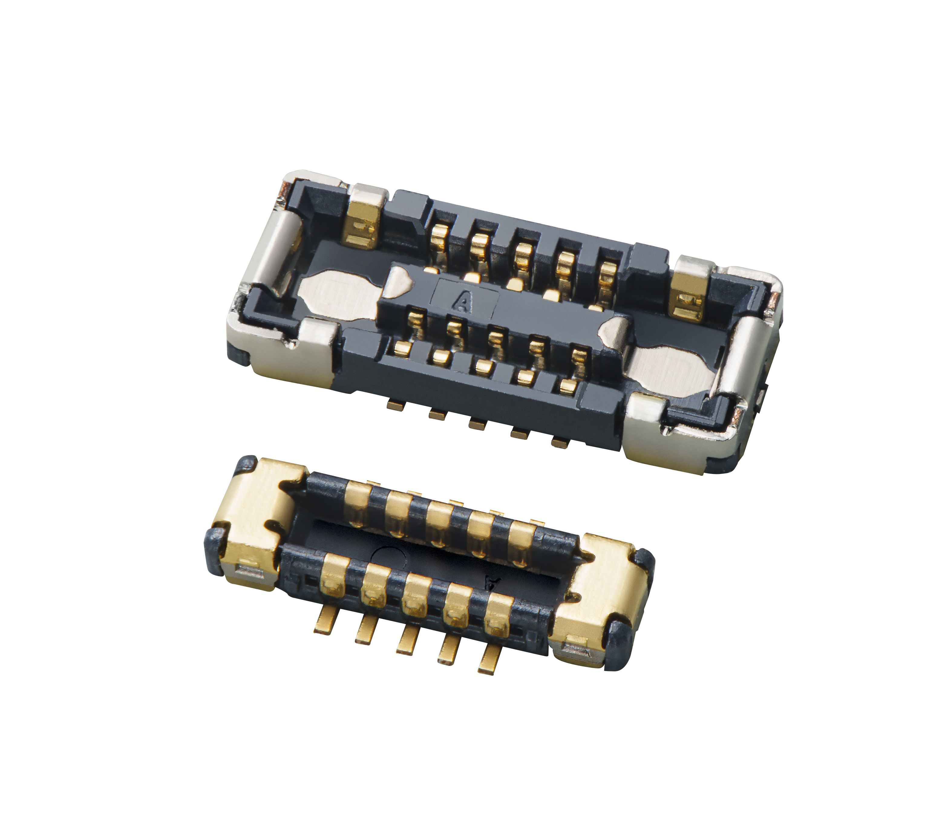
KYOTO, Japan--(BUSINESS WIRE)--Kyocera Corporation (President: Hideo Tanimoto, hereinafter: Kyocera)(TOKYO:6971) today released its new 5814 Series, a 0.3mm pitch Board-to-Board connector contributing to the miniaturization and expanding functionality of devices with its compact size*. The product is now available for general sale starting February 5th, 2024. This connector achieves industry-leading narrow pitch and compact dimensions, with a stacking height of 0.6mm and width of 1.5mm, and is designed to prevent damage during connector mating operations through its unique metal fitting structure.
*According to Kyocera's research in January 2024
Series |
5814 |
Pitch |
0.3mm |
Size |
Width: 1.5mm
|
No. of Positions |
10 to 50 |
Operating Temperature Range |
-40℃ to +85℃ |
Features |
1) Space-Saving Design
|
The accelerating trend towards miniaturization and higher functionality in communication terminals such as smartphones and tablet PCs, as well as wearable devices such as smartwatches and AR/VR glasses, requires a further reduction in the height and area of electronic components mounted on internal boards. This adds mounting complexity, especially in connectors that make board-to-board or board-to-FPC connections, which makes guiding structures increasingly necessary for damage prevention in the mating process.
Kyocera has commercialized the “5814 Series” Board to Board connectors to meet these market needs with a space-saving design and a unique damage-prevention structure.
This product can be used not only for board-to-board connection but also for board-to-FPC.
"5814 Series" Features
1) Space-Saving Design
Compared to our conventional product (0.35 mm pitch), it requires 32% less surface area.
- New Product: 0.30mm Pitch, Width 1.50mm
- Conventional product 0.35mm Pitch, Width 1.95mm
2) Structure Prevents Damage During Mating
The unique structure of two metal fitting parts, one on the outside and one on the inside of both ends, each suitable for a different function, improves guiding function during mating operations and reduces working time. Each fitting is soldered to the board to enhance strength against deformation and breakage.
3) Independent Power Supply Contacts
Apart from signal pins, two power supply pins at both ends can be energized to a DC 5A contact. Consequently, this feature enables compatibility with the increasing demand for rapid charging in smartphones and wearable devices.
For more information, please see:
https://ele.kyocera.com/en/technical/con_5814/
Contacts
KYOCERA Corporation (Japan) Corporate Communications
Head Office TEL: +81-(0)75-604-3416
E-mail: webmaster.pressgl@kyocera.jp