Enablence Technologies Ramps Capacity at Fremont Fab – Announces Strategic Partnership with Semiconductor Specialty Services Foundry, Noel Technologies
Enablence Technologies Ramps Capacity at Fremont Fab – Announces Strategic Partnership with Semiconductor Specialty Services Foundry, Noel Technologies
Enablence Enters Strategic Partnership Designed to Increased Customer Demand Across its Datacoms and Active Vision Business Units
FREMONT, Calif.--(BUSINESS WIRE)--Enablence Technologies Inc. (“Enablence”) (TSX-V: ENA), a leading supplier of photonics semiconductors used by the world’s top transceiver companies and Noel Technologies, a Pure Wafer company, and a leading supplier of advanced semiconductor process development and fabrication services to global semiconductor manufacturers and their OEMs announced today a strategic partnership designed to substantially ramp production of Enablence’s planar lightwave products at its Fremont, California wafer fab.
Enablence and Noel Technologies are making investments in etching, lithography and deposition processing technologies designed to increase production of Enablence’s planar lightwave circuits (PLCs). PLC demand has skyrocketed recently, driven by bourgeoning demand for data center and advanced vision applications where small footprint, performance, high efficiency optical solutions provide major benefits over more expensive and limiting technologies. With a roadmap fully established, Enablence’s planar light wave circuit (PLC) technology provides a higher volume of optical component integration in an ever-decreasing footprint, offering lower cost, lower power, higher-capacity advantages for systems using wavelength-division multiplexing and coherent sensing applications.
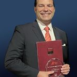
“In recent months, we have been experiencing increased interest and demand for our products and expertise from multinationals in a variety of end markets that fit within our key verticals. Our partnership with Noel will serve as a first step in supporting an accelerated growth phase for Enablence,” noted Todd Haugen, CEO, Enablence. “Noel’s proven experience in demanding photonics applications coupled with its deep semiconductor processing expertise will enable us to accelerate our technology roadmap, increase yields and quickly meet our production goals,” added Haugen.
“We are excited to work with Enablence to support the production ramp of their optical chip products,” commented S. Mark Borowicz, CEO, Pure Wafer, and Noel Technologies. “Our investments in advanced technologies and our 26-year track record helping customers quickly move prototyping projects from development to full production across a broad range of applications, continues to increase demand for our services and helps us to accelerate our continuing growth plans.”
About Noel Technologies
Noel Technologies is a Pure Wafer company based in Campbell, California. Its innovative process development and engineering optimization solutions meet the needs of the world’s top fabless semiconductor companies, OEMs, and IDMs. Visit Noel Technologies or connect via email info@noeltech.com.
Pure Wafer is America’s number one supplier of silicon wafer solutions and services to the global semiconductor industry. Operating three semiconductor fabs in California and Arizona, Pure Wafer supplies a comprehensive range of silicon wafer solutions, including prime grade silicon wafer reclaim, from 50mm to 300mm. Pure Wafer is also the official exclusive worldwide seller of films for Lam Research Corporation. For more information, visit Pure Wafer
About Enablence
Enablence is a publicly traded company listed on the TSX Venture Exchange ("TSX-V" - ENA) that designs, manufactures, and sells optical components, primarily in the form of planar lightwave circuits (PLC), on silicon-based chips. Enablence products serve a global customer base, primarily focused today on data center and other rapidly growing end markets. Enablence also works with customers that have emerging market uses for its technology, including medical devices, automotive LiDAR, and virtual and augmented reality headsets. In select strategic circumstances, the Company also uses its proprietary, non-captive fabrication plant in Fremont, California to manufacture chips designed by third party customers. For more information, visit: www.enablence.com. Or email Sales-ENA@enablence.com
Cautionary Note Regarding Forward-Looking Information
This news release contains forward-looking statements regarding Enablence based on current expectations and assumptions of management, which involve known and unknown risks and uncertainties associated with our business and the economic environment in which the business operates. All such statements are forward-looking statements under applicable Canadian securities legislation. Any statements contained herein that are not statements of historical facts may be deemed to be forward-looking statements. By their nature, forward-looking statements require us to make assumptions and are subject to inherent risks and uncertainties. These statements are based on current expectations that involve several risks and uncertainties which could cause actual results to differ from those anticipated. Although Enablence believes that the expectations reflected in the forward-looking statements contained in this news release, and the assumptions on which such forward-looking statements are made, are reasonable, there can be no assurance that such expectations will prove to be correct. We caution our readers of this news release not to place undue reliance on our forward-looking statements as a number of factors could cause actual results or conditions to differ materially from current expectations. Additional information on these and other factors that could affect Enablence’s operations are set forth in its continuous disclosure documents that can be found on SEDAR (www.sedar.com) under Enablence's issuer profile. Enablence does not intend, and disclaims any obligation, except as required by law, to update or revise any forward-looking statements whether as a result of new information, future events or otherwise.
Neither TSX Venture Exchange nor its Regulation Services Provider (as that term is defined in the policies of the TSX Venture Exchange) accepts responsibility for the adequacy or accuracy of this release. No stock exchange, securities commission or other regulatory authority has approved or disapproved the information contained herein.
Contacts
Hill & Kincaid Marketing & PR
Press@hillandkincaid.com