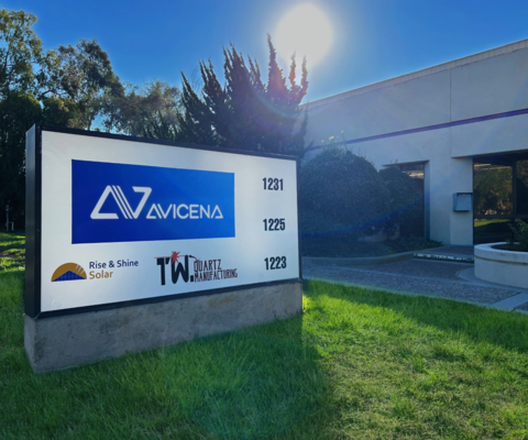
Avicena Acquires microLED Fab Facility and Engineering Team From Nanosys
Avicena Acquires microLED Fab Facility and Engineering Team From Nanosys
Avicena enhances its leadership position in microLED-based multi-Tbps chip-to-chip interconnects through the acquisition of a microLED fab facility and engineering team from Nanosys
MOUNTAIN VIEW, Calif.--(BUSINESS WIRE)--Avicena, the leader in high-performance microLED-based chip-to-chip interconnects, today announced that it has completed the acquisition of a microLED fabrication facility and associated engineering team from Nanosys. This transaction significantly enhances Avicena’s capabilities in the development and manufacturing of high-speed GaN microLEDs optimized for parallel multi-Tbps interconnects.
The GaN microLED fab was previously owned by glō, which invested over $200 million in the development of best-in-class microLED displays including very significant investments in manufacturing capabilities. Nanosys acquired glō in May 2021. Avicena had been using the Nanosys fab for the development of unique ultra-fast microLEDs. The acquisition of the fab and associated engineering team significantly increases the development and manufacturing capabilities.
“We have already demonstrated LightBundle™ links running at less than 1pJ/bit and individual microLED links running at 14Gbps NRZ,” says Bardia Pezeshki, founder and CEO of Avicena, “With the acquisition of the Nanosys microLED development facilities we will be in an excellent position to further advance epitaxy, device process and transfer technology and achieve even lower energy and higher data rates per lane. Compact, low-cost interconnects using hundreds of these links can support a total bandwidth of many terabits per second and help solve the data bottleneck in advanced silicon ICs.”
The facilities include state-of-the-art epitaxy, wafer processing, and lift-off and transfer tools to post-process silicon ICs with optical interfaces. Together with Avicena’s internal ASIC team, the company plans to deliver optical chiplets with high capacity and extremely low power. Compared to laser or silicon photonics-based interconnects, microLED optical interconnects are well-suited for integration with silicon ICs, lower power, lower cost, and target reaches up to 10m.
“We thank the microLED fab team for their partnership in developing and manufacturing microLEDs as part of Nanosys and wish them well in their future with Avicena,” said Jason Hartlove, President and CEO of Nanosys. “Avicena is an exciting company developing cutting-edge microLED solutions, and we are pleased to have an equity stake and the opportunity to continue to collaborate with them during their next phase of growth.”
About Avicena’s LightBundle™ Technology
LightBundle™ is based on arrays of innovative ultra-fast GaN microLEDs that leverage the microLED display ecosystem and can be integrated directly onto high performance CMOS ICs. Each ultra-low power microLED array is connected via a multi-core fiber cable using hundreds of parallel optical lanes to a matching array of CMOS-compatible PDs. This design enables ultra-low power, low-cost multi-Tbps interconnects with up to 10m reach.
Interconnects have become the key bottleneck in modern compute and networking systems. Highly variable workloads are driving the evolution of densely interconnected, heterogeneous, software-defined clusters of XPUs, Smart NICs, hardware accelerators, and high-performance shared memory. Ever growing Artificial Intelligence (AI)/Machine Learning (ML) and High-Performance Computing (HPC) workloads are driving the need for interconnects with ultra-high bandwidth density, ultra-low power consumption, and low latency.
The parallel nature of LightBundle™ is well-matched to parallel chiplet interfaces like UCIe, OpenHBI, and BoW, and can also be used to extend the reach of existing compute interconnects like PCIe/CXL, and HBM/DDR/GDDR memory links, as well as various inter-processor interconnects like NVLink with low power and low latency.
About Avicena
Avicena is a privately held company located in Mountain View, CA, developing ultra-low energy optical links based on microLEDs. These interconnects offer class-leading bandwidth density and energy efficiency for medium reach. Applications include chip-to-chip interconnects in HPC, AI/ML, and memory disaggregation, as well as next generation links in sensors, 5G wireless and aerospace. Avicena’s technology is a key building block in the evolution of new networking and computing architectures that will reduce the energy impact on our planet.
For more information, visit: https://www.avicena.tech
About Nanosys, Inc.
Nanosys, Inc. is the leader in developing and delivering quantum dot technology to the display industry. As of 2022, industry-leading consumer electronics brands have shipped more than 60 million devices in over 900 unique products from tablets to monitors and TVs based on Nanosys’ proprietary quantum dot technology. Founded in 2001, the company is headquartered in Silicon Valley, California where it operates the world’s largest quantum dot nanomaterials fab. Nanosys owns or has exclusive license rights to more than 900 issued and pending patents worldwide.
For more information, visit https://www.nanosys.com
Contacts
Nanosys Contact:
Jeff Yurek, (781) 801-0029, jyurek@nanosysinc.com
Avicena Contact:
Sama Pourmojib, sama@avicena.tech

