New Cadence Certus Delivers Up to 10X Faster Concurrent Full-Chip Optimization and Signoff
New Cadence Certus Delivers Up to 10X Faster Concurrent Full-Chip Optimization and Signoff
Highlights:
- Provides customers with a first-of-its-kind fully automated environment featuring a massively parallel and distributed architecture
- Supports design optimization and signoff with unlimited capacity, delivering overnight turnaround time while significantly reducing design power
- Cloud-ready solution advances emerging design areas, including hyperscale computing, 5G communications, mobile, automotive and networking
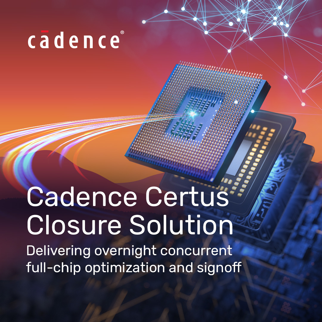
SAN JOSE, Calif.--(BUSINESS WIRE)--Cadence Design Systems, Inc. (Nasdaq: CDNS) today announced the new Cadence® Certus™ Closure Solution to address growing chip-level design size and complexity challenges. The Cadence Certus Closure Solution environment automates and accelerates the complete design closure cycle from weeks to overnight—from signoff optimization through routing, static timing analysis (STA) and extraction. The solution supports the largest chip design projects with unlimited capacity while substantially improving productivity by up to 10X versus current methodologies and flows.
The Cadence Certus Closure Solution eases the design signoff closure bottlenecks and complexities that come with developing today’s emerging applications like hyperscale computing, 5G communications, mobile, automotive and networking. Prior to the introduction of the Cadence Certus Closure Solution, a full-chip closure flow involved manual, tedious processes from full chip assembly, static timing analysis, and optimization and signoff with 100s of views, taking designers months to converge. The new solution provides a fully automated environment that is massively distributed for superior optimization and signoff. This allows concurrent, full-chip optimization through an engine shared with Cadence’s Innovus™ Implementation System and the Tempus™ Timing Signoff Solution, eliminating iterative loops with block owners while enabling designers to make quick optimization and signoff decisions. Furthermore, in conjunction with the Cadence Cerebrus™ Intelligent Chip Explorer, designers can experience additional productivity improvements from block-level to full-chip signoff closure.
The Cadence Certus Closure Solution provides customers with the following benefits:
- Innovative scalable architecture: The Cadence Certus Closure Solution’s distributed hierarchical optimization and signoff architecture is ideal for cloud-execution and is operational in both cloud and internal data center environments
- Incremental signoff: Provides flexible restore and replacement of only the changed portions of the design, further accelerating final signoff
- Improved engineering productivity: Fully automated flow reduces the need for multiple, lengthy iterations across multiple teams, providing faster time-to-market
- SmartHub interface: Enhanced interactive GUI allows cross-probing for detailed timing debug to drive last-mile design closure
- 3D-IC design efficiencies: Tightly integrated with the Cadence Integrity™ 3D-IC Solution, it allows users to close inter-die paths across heterogenous process dies
“Today’s design teams often spend five to seven days per iteration to meet chip-level signoff timing and power requirements, and previous methodologies failed to deliver the team collaboration and user experience needed for efficient design closure,” said Dr. Chin-Chi Teng, senior vice president and general manager in the Digital & Signoff Group at Cadence. “We are intensely in tune with the needs of the design community, and with the release of the new Cadence Certus Closure Solution, we’re offering our customers a novel environment for chip-level optimization and signoff that delivers exceptional PPA results within a matter of hours. With this new Cadence solution, we’re empowering customers to achieve productivity goals and deliver products to market faster.”
The Cadence Certus Closure Solution supports the company’s Intelligent System Design™ strategy, which enables design excellence. For more information, please visit www.cadence.com/go/certuspr.
Customer Endorsements
“It is imperative for us to deliver our high-performance and low-power analog and mixed-signal products on schedule. Full chip-level signoff closure is one of the biggest bottlenecks our engineering team faces when working tirelessly to meet customer delivery commitments. With the Cadence Certus Closure Solution, our engineering team can experience overnight full chip-level signoff closure via its concurrent optimization and signoff capabilities, improving overall engineering team productivity. The solution’s ability to automate the whole optimization and signoff flow—STA, routing, and extraction—empowers our engineering team to achieve greatly improved design success, realize untapped power savings of up to 5% and get to market faster.”
-Dr. Paolo Miliozzi, vice president, SoC Design and Technology, MaxLinear
“In today’s dynamic design environment, we require automated and robust signoff closure methodologies and tools to meet time-to-market objectives. With the Cadence Certus Closure Solution, our engineering team observed 6X faster chip-level signoff closure turnaround time versus current methodologies, improving overall productivity. Following this success, we plan to adopt the solution for the development of our latest designs.”
-Yukio Minoda, Senior Principal Engineer, Digital Design Technology Department, Shared R&D EDA Division, Renesas
About Cadence
Cadence is a pivotal leader in electronic systems design, building upon more than 30 years of computational software expertise. The company applies its underlying Intelligent System Design strategy to deliver software, hardware and IP that turn design concepts into reality. Cadence customers are the world’s most innovative companies, delivering extraordinary electronic products from chips to boards to complete systems for the most dynamic market applications, including hyperscale computing, 5G communications, automotive, mobile, aerospace, consumer, industrial and healthcare. For eight years in a row, Fortune magazine has named Cadence one of the 100 Best Companies to Work For. Learn more at cadence.com.
© 2022 Cadence Design Systems, Inc. All rights reserved worldwide. Cadence, the Cadence logo and the other Cadence marks found at www.cadence.com/go/trademarks are trademarks or registered trademarks of Cadence Design Systems, Inc. All other trademarks are the property of their respective owners.
Category: Featured
Contacts
Cadence Newsroom
408-944-7039
newsroom@cadence.com