Kyocera to Build Its Largest Plant in Japan, Increasing Production of Semiconductor Components
Kyocera to Build Its Largest Plant in Japan, Increasing Production of Semiconductor Components
Expanded Sendai Plant Campus in Kagoshima will meet increasing demand for semiconductor packages powering ADAS, sensor cameras, 5G and more

KYOTO, Japan--(BUSINESS WIRE)--Kyocera Corporation (hereinafter “Kyocera;” President: Hideo Tanimoto) today announced a plan to build the largest manufacturing facility it has ever operated in Japan, expanding production capacity for components including organic semiconductor packages and crystal device packages. A signing ceremony held April 20, 2022 was attended by Kagoshima Governor Koichi Shiota, Satsumasendai City Mayor Ryoji Tanaka, and Kyocera officials. Construction is scheduled to begin next month at the company’s Sendai Plant Campus in Kagoshima.
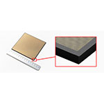
Three converging factors are creating strong demand for Kyocera’s organic semiconductor packages and crystal device packages. Smart vehicles are expanding the need for automotive cameras and high-performance processors used in Advanced Driver-Assistance Systems (ADAS) and autonomous driving. New communications infrastructures, including fifth-generation (5G) base stations and datacenters, are being deployed worldwide. In addition, the rising trend toward digitalization is expanding demand for electronic products ranging from personal computers and smartphones to consumer goods, industrial automation, and others.
Kyocera will open the new facility in October 2023 to serve these growing trends, aiming for a 4.5-fold increase in production capacity for organic packages at the Sendai Plant Campus, as well as a substantial increase in capacity for crystal device packages.
Kyocera will contribute to the community by stimulating economic development in Kagoshima, creating new employment opportunities through expanded production of semiconductor components in response to global demand.
Outline of New Facility
Name |
Plant No.23 at Kyocera’s Kagoshima Sendai Campus |
Address |
2310-10 Taki-cho, Satsumasendai-shi, Kagoshima Prefecture, Japan |
Total investment |
Approximately 62.5 billion yen (approx. 488 million U.S. dollars) |
Building footprint |
12,380 m2 (133,257 f2), steel construction, 6 stories |
Total area |
65,530 m2 (705,359 f2) |
Construction plan |
Construction to begin May 2022 Facility to open October 2023 |
Production items |
Organic packages, crystal device packages |
Expected production level |
Approximately 33 billion yen (approx. 258 million U.S. dollars) per year (April 2024-March 2025) |
Kyocera Corporation (TOKYO:6971, https://global.kyocera.com/), the parent and global headquarters of the Kyocera Group, was founded in 1959 as a producer of fine ceramics (also known as “advanced ceramics”). By combining these engineered materials with metals and integrating them with other technologies, Kyocera has become a leading supplier of industrial and automotive components, semiconductor packages, electronic devices, smart energy systems, printers, copiers, and mobile phones. During the year ended March 31, 2021, the company’s consolidated sales revenue totaled 1.5 trillion yen (approx. US$13.8 billion). Kyocera is ranked #603 on Forbes magazine’s 2021 “Global 2000” list of the world’s largest publicly traded companies, and has been named by The Wall Street Journal among “The World’s 100 Most Sustainably Managed Companies.”
Contacts
KYOCERA Corporation (Japan), Corporate Communications
Kenichi Hara, Tel: +81-(0)75-604-3514 Fax: +81-(0)75-604-3516
webmaster.pressgl@kyocera.jp