Keysight EDA and Intel Foundry Collaborate on EMIB-T Silicon Bridge Technology for Next-Generation AI and Data Center Solutions
Keysight EDA and Intel Foundry Collaborate on EMIB-T Silicon Bridge Technology for Next-Generation AI and Data Center Solutions
- Supports latest interconnect standards, including Universal Chiplet Interconnect Express™ 2.0 and Open Compute Project Bunch of Wires, for improved design flexibility
- Enhances Keysight’s EDA standards-based approach, enabling high-speed digital chiplet design and supporting EMIB-T tailored for AI and data center markets
SANTA ROSA, Calif.--(BUSINESS WIRE)--Keysight Technologies, Inc. (NYSE: KEYS) announced today a collaboration with Intel Foundry to support Embedded Multi-die Interconnect Bridge-T (EMIB-T) technology, a cutting-edge innovation aimed at improving high-performance packaging solutions for artificial intelligence (AI) and data center markets in addition to the support of Intel 18A process node.
As the demands of AI and data center workloads continue to grow in complexity, ensuring reliable communication between chiplets and 3DICs is becoming increasingly critical. High-speed data transfer and efficient power delivery are essential to meet the performance demands of next-generation semiconductor applications. The semiconductor industry addresses these challenges through emerging open standards, such as Universal Chiplet Interconnect Express™ (UCIe™) and Bunch of Wires (BoW). These standards define interconnect protocols for chiplets and 3DICs within advanced 2.5D/3D or laminate/organic packages, enabling consistent, high-quality integration across different design platforms.
By adopting these standards and verifying chiplets for compliance and link margin, Keysight EDA and Intel Foundry contribute to a growing chiplet interoperability ecosystem. The collaboration aims to reduce development costs, mitigate risk, and accelerate innovation in semiconductor design.
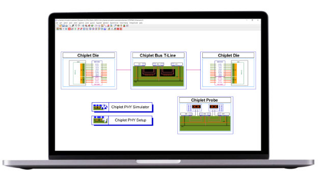
Keysight EDA’s Chiplet PHY Designer, the latest solution for high-speed digital chiplet design tailored to AI and data center applications, now offers advanced simulation capabilities for the UCIe™ 2.0 standard and introduces support for the Open Computer Project BoW standard. As an advanced, system-level chiplet design and die-to-die (D2D) design solution, Chiplet PHY Designer enables pre-silicon level validation, streamlining the path to tapeout.
Suk Lee, VP & GM of Ecosystem Technology Office, Intel Foundry, said: “Our collaboration with Keysight EDA on EMIB-T silicon bridge technology is a pivotal step in advancing high-performance packaging solutions. By integrating standards like UCIe™ 2.0, we enhance chiplet design flexibility for AI and data center applications, accelerating innovation and ensuring our customers meet next-generation demands with precision.”
Niels Faché, Vice President and General Manager, Keysight’s Design Engineering Software, said: "Keysight EDA's pioneering Chiplet PHY Designer continues to redefine pre-silicon validation, empowering chiplet designers with rapid, accurate verification. By proactively embracing evolving standards like UCIe 2.0 and BoW, and now with critical support for Intel Foundry’s EMIB-T, we're enabling engineers to accelerate innovation and eliminate costly design iterations before manufacturing."
See Keysight EDA EMIB-T Solution at Intel Foundry Direct Connect
Keysight will demonstrate its EMIB-T workflow for system-level link performance and compliance, featuring Intel Foundry’s EMIB-T technology, at Intel Foundry Direct Connect on April 29th in San Jose.
Resources:
About Keysight Technologies
At Keysight (NYSE: KEYS), we inspire and empower innovators to bring world-changing technologies to life. As an S&P 500 company, we deliver market-leading design, emulation, and test solutions to help engineers develop and deploy faster, with less risk, throughout the entire product life cycle. We’re a global innovation partner enabling customers in communications, industrial automation, aerospace and defense, automotive, semiconductor, and general electronics markets to accelerate innovation to connect and secure the world. Learn more at Keysight Newsroom and www.keysight.com.
Contacts
Keysight Media Contacts
Andrea Mueller
Americas
Andrea.mueller@keysight.com
Fusako Dohi
Asia
+81 42 660-2162
fusako_dohi@keysight.com
Jenny Gallacher
Europe
+44 (0) 7800 737 982
jenny.gallacher@keysight.com