Avicena Works with TSMC to Enable PD Arrays for LightBundle™ MicroLED-Based Interconnects
Avicena Works with TSMC to Enable PD Arrays for LightBundle™ MicroLED-Based Interconnects
Avicena is working with TSMC to optimize silicon photodetector (PD) arrays for Avicena’s LightBundle microLED-based interconnects aimed at AI scale-up networks with > 1Tbps/mm I/O density and < 1pJ/bit efficiency.
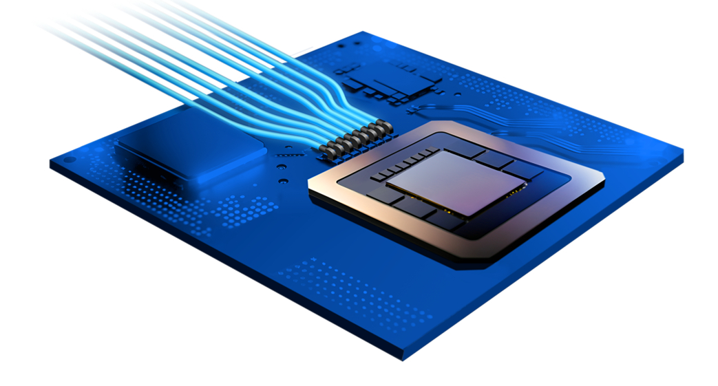
SUNNYVALE, Calif.--(BUSINESS WIRE)--Avicena, headquartered in Sunnyvale, CA, announced today that the company will work with TSMC to optimize photodetector (PD) arrays for Avicena’s revolutionary LightBundle microLED-based interconnects. LightBundle supports > 1Tbps/mm shoreline density and extends ultra-high density die-to-die (D2D) connections to > 10 meters at class-leading sub-pJ/bit energy efficiency. This will enable AI scale-up networks to support large clusters of GPUs across multiple racks, eliminating reach limitations of current copper interconnects while drastically reducing power consumption.
Increasingly sophisticated AI models are driving an unprecedented surge in demand for compute and memory performance, requiring interconnects with higher density, lower power, and longer reach for both processor-to-processor (P2P) and processor-to-memory (P2M) connectivity.
LightBundle technology has been developed specifically to address extreme I/O requirements of AI clusters with extremely high shoreline densities and ultra-low power consumption. LightBundle transmitters use microLED arrays optimized for dense, high-speed interconnects achieving < 1pJ/bit energy efficiency. LightBundle optical receivers utilize silicon PD arrays optimized for the visible light wavelengths transmitted by the microLEDs. LightBundle chiplet transceivers are well-suited to various packaging architectures including co-packaged optics (CPO), on-board optics (OBO), and pluggable optical modules. Both LED and PD arrays are bonded directly to the surface of CMOS ICs for a variety of process nodes. This work harnesses TSMC’s leadership in image and optic sensor technologies to produce high-performance PD arrays for visible light, while also benefiting from TSMC’s manufacturing excellence.
“Avicena has been working with TSMC since our very beginning. TSMC’s world-class manufacturing capabilities and deep experience in silicon optical sensors are critical for developing and producing key components of our LightBundle interconnects,” says Bardia Pezeshki, co-founder and CEO of Avicena.
“We are delighted to collaborate with innovators like Avicena to advance AI infrastructure, addressing the growing demands for compute scalability through efficient connectivity,” said Lucas Tsai, Vice President of Business Management at TSMC North America. “TSMC provides foundry’s most comprehensive CMOS image sensor (CIS) technology portfolio, and we’re excited to support Avicena with our leading processes and manufacturing expertise.”
Avicena will exhibit in the Innovation Zone at the TSMC 2025 North America Technology Symposium in Santa Clara, CA, where it will showcase its LightBundle interconnect platform at Booth IZ09 and Co-Founder & CEO Bardia Pezeshki will present at the “Innovate with TSMC!” Forum.
About Avicena
Avicena Tech Corp. is a privately held company located in Sunnyvale, CA, developing LightBundle, a next generation optical interconnect architecture for AI/ML, HPC, sensors, 5G wireless and aerospace applications. This unique, flexible ultra-low energy technology is based on microLEDs, offering both very high bandwidth and low latency. Now, system designers can disaggregate functions like compute and memory and radically grow system throughput. Avicena’s technology is a key building block in the evolution of networking and computing that will reduce the energy impact on our planet.
For more information, visit https://avicena.tech
Contacts
Avicena Media Contact:
Sama Pourmojib
email: sama@avicena.tech