Samsung Reaches Key Milestone at New Semiconductor R&D Complex
Samsung Reaches Key Milestone at New Semiconductor R&D Complex
Samsung holds tool-in ceremony for NRD-K, scheduled to start operation in 2025
Samsung plans to invest about KRW 20 trillion by 2030 for advanced semiconductor R&D
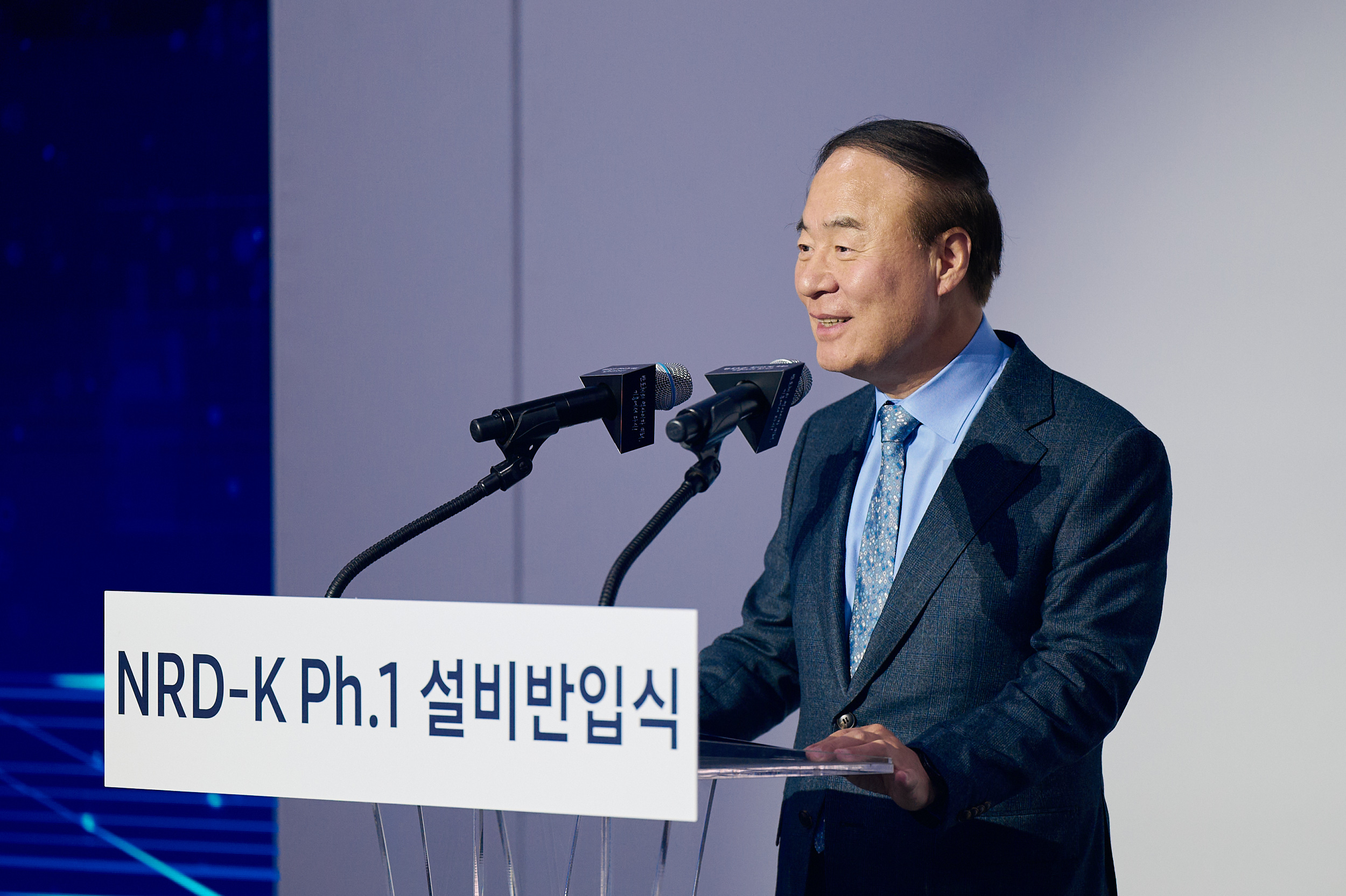
SEOUL, Korea--(BUSINESS WIRE)--Samsung Electronics Co., Ltd. today announced that it held a tool-in ceremony for its new semiconductor research and development complex (NRD-K) at its Giheung campus, marking a significant leap into the future. About 100 guests, including those from suppliers and customers, were in attendance to celebrate the milestone.
As a state-of-the-art facility, NRD-K broke ground in 2022 and is set to become a key research base for Samsung’s memory, system LSI and foundry semiconductor R&D. With its advanced infrastructure, research and product-level verification will be able to take place under one roof. Samsung plans to invest about KRW 20 trillion by 2030 for the complex in an area covering about 109,000 square meters (m2) within its Giheung campus. The complex will also include an R&D-dedicated line scheduled to begin operation in mid-2025.
"NRD-K will bolster our development speed, enabling the company to create a virtuous cycle to accelerate fundamental research on next generation technology and mass production. We will lay the foundation for a new leap forward in Giheung, where Samsung Electronics' 50-year history of semiconductors began, and create a new future for the next 100 years," said Young Hyun Jun, Vice Chairman and Head of the Device Solutions Division at Samsung Electronics.
"At a time when the importance of win-win partnerships is greater than ever, Applied Materials is committed to accelerating innovation velocity through deep collaboration with Samsung Electronics, working together to drive a new wave of growth for the semiconductor industry," said Park Gwang-Sun, head of Applied Materials Korea.
Samsung’s Giheung campus, located south of Seoul, is the birthplace of the world’s first 64-megabit (Mb) DRAM in 1992, marking the beginning of the company’s semiconductor leadership. The establishment of the new R&D facility will usher in the latest developments in process technology and manufacturing tools, extending the site’s legacy at the forefront of innovation.
NRD-K will be set up with High NA extreme ultra-violet (EUV) lithography and new material deposition equipment aimed at accelerating the development of next-generation memory semiconductors such as 3D DRAM and V-NAND with more than 1,000 layers. In addition, wafer bonding infrastructure with innovative wafer-to-wafer bonding capabilities are also planned to dock.
Samsung invested a record KRW 8.87 trillion in R&D in the third quarter of this year, and continues to push boundaries to secure competitiveness in future technologies, such as advanced packaging for high bandwidth memory (HBM) production.
About Samsung Electronics Co., Ltd.
Samsung inspires the world and shapes the future with transformative ideas and technologies. The company is redefining the worlds of TVs, smartphones, wearable devices, tablets, home appliances, network systems, and memory, system LSI, foundry and LED solutions, and delivering a seamless connected experience through its SmartThings ecosystem and open collaboration with partners. For the latest news, please visit the Samsung Newsroom at news.samsung.com.
Contacts
Ujeong Jahnke
Samsung Semiconductor Europe GmbH
Tel. +49(0)89-45578-1000
Email: sseg.comm@samsung.com