Samsung Begins Industry's First Mass Production of QLC 9th-Gen V-NAND for AI Era
Samsung Begins Industry's First Mass Production of QLC 9th-Gen V-NAND for AI Era
Latest QLC V-NAND combines several breakthrough technologies, including Channel Hole Etching that enables the highest layer count in the industry with double stack structure
Industry-first QLC and TLC 9th-gen V-NAND delivers optimum memory across various AI applications
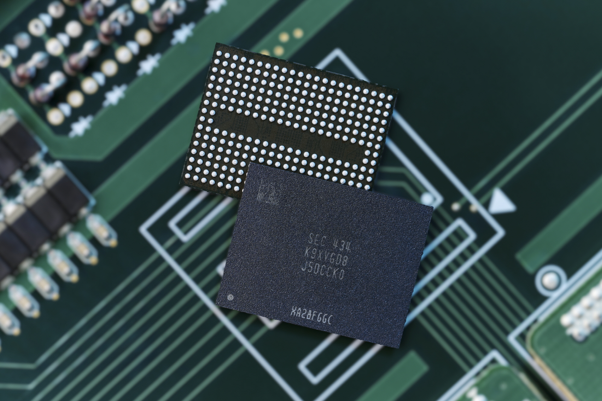
SEOUL, South Korea--(BUSINESS WIRE)--Samsung Electronics Co., Ltd., the world leader in advanced memory technology, today announced it has begun mass production of its one-terabit (Tb) quad-level cell (QLC) 9th-generation vertical NAND (V-NAND).
With the industry’s first mass production of QLC 9th-generation V-NAND, following the industry’s first triple-level cell (TLC) 9th-generation V-NAND production in April this year, Samsung is solidifying its leadership in the high-capacity, high-performance NAND flash market.
“Kicking off the successful mass production of QLC 9th-generation V-NAND just four months after the TLC version allows us to offer a full lineup of advanced SSD solutions that address the needs for the AI era,” said SungHoi Hur, Executive Vice President and Head of Flash Product & Technology at Samsung Electronics. “As the enterprise SSD market shows rapid growth with stronger demand for AI applications, we will continue to solidify our leadership in the segment through our QLC and TLC 9th-generation V-NAND.”
Samsung plans to expand applications of the QLC 9th-generation V-NAND, starting with branded consumer products and extending into mobile Universal Flash Storage (UFS), PCs and server SSDs for customers including cloud service providers.
Samsung's QLC 9th-generation V-NAND brings together a number of innovations that have produced technological breakthroughs:
- Samsung’s unrivaled Channel Hole Etching technology was used to achieve the highest layer count in the industry with a double stack structure. Utilizing the technological expertise gained from the TLC 9th-generation V-NAND, the area of the cells and the peripheral circuits have been optimized, achieving an industry-leading bit density approximately 86% higher than that of the previous generation QLC V-NAND.
- Designed Mold technology adjusts the spacing of Word Lines (WL), which operate the cells, to ensure uniformity and optimization of cell characteristics across and within layers. These traits have become increasingly important as the V-NAND layer counts increase. Adopting Designed Mold has improved data retention performance by roughly 20% compared to previous versions, leading to enhanced product reliability.
- Predictive Program technology anticipates and controls cell state changes to minimize unnecessary actions. Samsung’s QLC 9th-generation V-NAND has doubled write performance and improved data input/output speed by 60% through advancements to this technology.
- Data read and write power consumption decreased by about 30% and 50% respectively, with the use of Low-Power Design technology. This method reduces the voltage that drives NAND cells and minimizes power consumption by sensing only the necessary bit lines (BL).
About Samsung Electronics Co., Ltd.
Samsung inspires the world and shapes the future with transformative ideas and technologies. The company is redefining the worlds of TVs, smartphones, wearable devices, tablets, home appliances, network systems, and memory, system LSI, foundry and LED solutions, and delivering a seamless connected experience through its SmartThings ecosystem and open collaboration with partners. For the latest news, please visit the Samsung Newsroom at news.samsung.com.
Contacts
Ujeong Jahnke
Samsung Semiconductor Europe GmbH
Tel. +49(0)89-45578-1000
Email: sseg.comm@samsung.com