Samsung Electronics Unveils Automotive Process Strategy at Samsung Foundry Forum 2023 EU
Samsung Electronics Unveils Automotive Process Strategy at Samsung Foundry Forum 2023 EU
Samsung Foundry meets with customers and partners in the European market at annual event in Munich
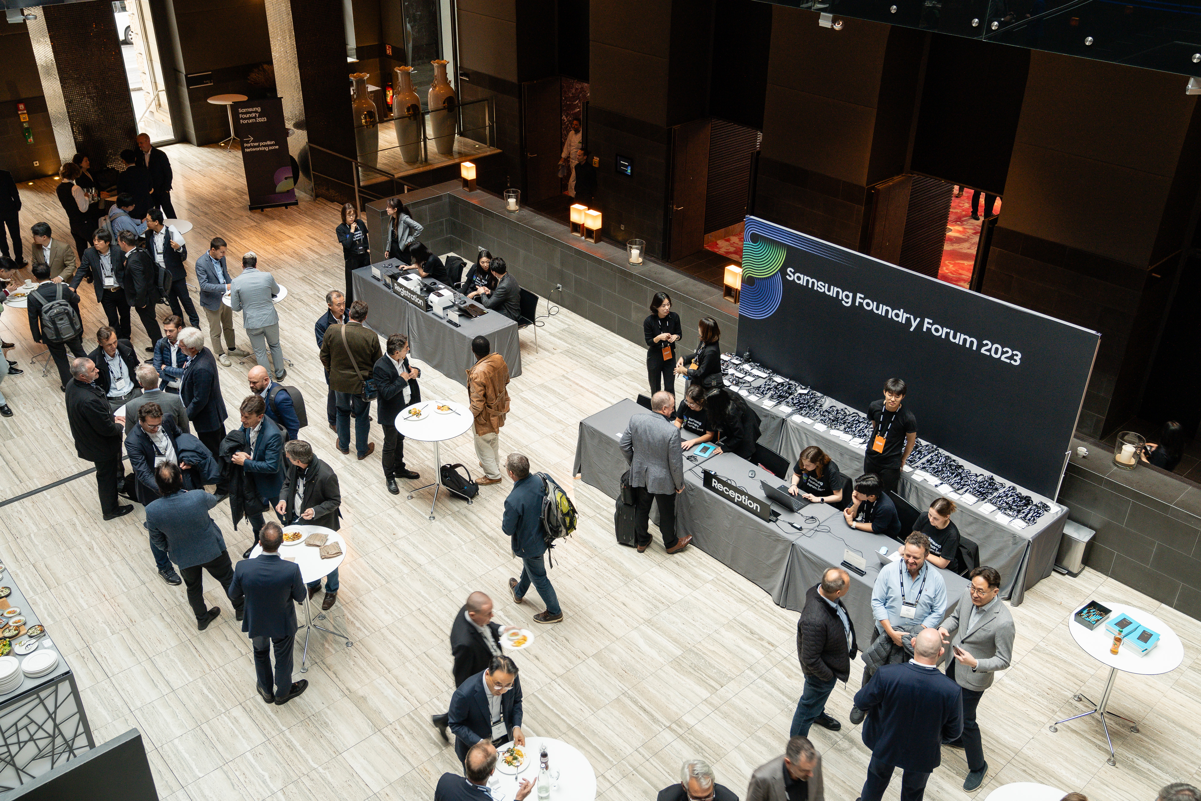
MUNICH--(BUSINESS WIRE)--Samsung Electronics Co., Ltd., a world leader in advanced semiconductor technology, today hosted Samsung Foundry Forum (SFF) 2023 Europe and unveiled its advanced and wide ranging automotive process solutions, from the most advanced 2-nanometer process to the 8-inch legacy process.
Alongside its customers and Samsung Advanced Foundry Ecosystem (SAFE) partners, Samsung Electronics showcased the latest technological trends and its business strategy tailored to the European market.
“Samsung Foundry is driving innovation in next-generation solutions to build an expanded portfolio that meets the growing needs of our automotive customers, especially as the era of electric vehicles becomes a reality,” said Dr. Siyoung Choi, President and Head of Foundry Business at Samsung Electronics. “We are strengthening our readiness to provide customers with distinguished service across a variety of solutions, including power semiconductors, microcontrollers and advanced AI chips for autonomous driving.”
Since participating in IAA Mobility 2023 for the first time in September, Samsung Electronics is strengthening engagement and partnership in specialty processes for automotive customers in the European market, further solidifying its status as a leading foundry partner for the industry.
Pioneering New Applications with Industry’s Most Advanced eMRAM
In order to meet the needs of the latest advancements in the automotive market, Samsung is setting out to develop the industry’s first 5-nanometer eMRAM for next-generation automotive technology. eMRAM is a next-generation memory semiconductor used for automotive applications that enables high read and write speeds as well as superior heat resistance.
Since developing and mass producing the industry’s first 28nm FD-SOI1 based eMRAM in 2019, Samsung Electronics has been developing 14nm for the FinFET process based on AEC-Q100 Grade 1. Samsung Foundry plans to expand its eMRAM portfolio by adding 14nm by 2024, 8nm by 2026, and 5nm by 2027.
Samsung’s 8nm eMRAM shows potential to deliver a 30% increase in density and 33% increase in speed, compared to the 14nm process.
Tackling the Market with Automotive Process Solutions from Cutting-Edge to Legacy
The company announced its advanced process roadmap, highlighting its plans to complete mass production readiness for its 2nm process for automotive applications by 2026.
Samsung Electronics is also bolstering its readiness to serve customer needs by expanding its 8-inch BCD (Bipolar-CMOS-DMOS) process portfolio. The BCD process combines the strengths of three different process technologies: Bipolar (B), CMOS (C), and DMOS (D) on one chip and is most commonly used in the production of power semiconductors.
Samsung Electronics plans to expand its current 130nm automotive BCD process to add 90nm by 2025. The 90nm BCD process is expected to bring a 20% decrease in chip area compared to the 130nm process.
Implementing Deep Trench Isolation (DTI) technology, which reduces the distance between each transistor to maximize the performance of power semiconductors, Samsung Foundry will be able to apply a greater voltage of 120V instead of 70V to a wider range of applications. This will enable readiness to provide a process development kit (PDK) that implements 120V to the 130nm BCD process by 2025.
Leading ‘Beyond-Moore’ Innovation through Advanced Packaging Alliance
Samsung established a Multi-Die Integration (MDI) Alliance by collaborating with its SAFE partners as well as major players in memory, package substrate, and testing.
As part of an industry-wide partnership with 20 partners, Samsung is leading the development of 2.5D and 3D packaging solutions customized for all applications from automotive to high-performance computing (HPC).
Samsung Electronics hosted the annual Samsung Foundry Forum 2023 in the United States on June 27-28, in South Korea on July 4, and in Japan on October 17. The content from the forum will be available on the Samsung Semiconductor website for worldwide access to all visitors beginning November 2.
# # #
About Samsung Electronics Co., Ltd.
Samsung inspires the world and shapes the future with transformative ideas and technologies. The company is redefining the worlds of TVs, smartphones, wearable devices, tablets, digital appliances, network systems, and memory, system LSI, foundry, and LED solutions. For the latest news, please visit the Samsung Newsroom at news.samsung.com.
1 Fully Depleted Silicon On Insulator (FD-SOI) is a planar process technology that implements an impervious insulating film (SiO2) on top of a silicon wafer and builds transistors on top of it to minimize leakage.
Contacts
Ujeong Jahnke
Samsung Semiconductor Europe GmbH
Tel. +49(0)89-45578-1000
Email: sseg.comm@samsung.com