KYOCERA to Increase MLCC Production for 5G, ADAS and EV Technology with New Manufacturing Plant
KYOCERA to Increase MLCC Production for 5G, ADAS and EV Technology with New Manufacturing Plant
Expanded multilayer ceramic capacitor production at Kagoshima Kokubu Campus in Japan will help meet strong market demand, increased production slated to begin in 2024
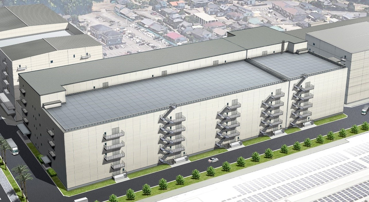
KYOTO, Japan--(BUSINESS WIRE)--Kyocera Corporation (President: Hideo Tanimoto, hereinafter “Kyocera”) announced today that it will construct a new production facility at its Kokubu Plant Campus in Kagoshima, Japan, to increase its production capacity of multilayer ceramic capacitors (MLCCs), strengthen engineering development capabilities, and ensure ample manufacturing space as Kyocera’s business expands.
Demand for MLCCs is expected to grow as communication terminals and semiconductor devices become more compact and sophisticated. Additionally, the expanding commercialization of 5G data centers, ADAS (advanced driver assistance systems) and EV (electric vehicle) technology will be facilitated by smaller, more functional electronic components like MLCCs.
A signing ceremony held on August 17, 2022 included Kagoshima Governor Koichi Shiota, Kirishima City Mayor Shinichi Nakashige, and Kyocera officials. Construction will begin in February 2023 and the plant will begin operation in May 2024. The new plant will be located on the current site of Kyocera’s Monozukuri R&D Laboratory, which will be demolished in September, 2022.
In addition to enhancing its electronic components business, Kyocera aims to stimulate economic development in Kagoshima Prefecture and to create new employment opportunities in the community.
▪Outline of New Facility |
|
Name |
Plants No. 5-1-2 at Kyocera’s Kagoshima Kokubu Plant Campus |
Address |
1-1 Kokubuyamashita-cho, Kirishima-shi, Kagoshima Prefecture, Japan |
Total investment |
Approximately 15 billion yen (approx. USD111 million) |
Building footprint |
7,197 m2 (77,468 f2), steel construction, 6 stories |
Total floor area |
37,600 m2 (404,723 f2) |
Construction plan |
Construction to begin: February 2023 Operation to begin: May 2024 |
Production items |
Multilayer ceramic capacitors (MLCC) and more |
Expected production level |
From May 2024 through March 2025: Approximately 10 billion yen (approx. USD74 million) per year FY2026: Approximately 20 billion yen (approx. USD148 million) thereafter |
Kyocera Corporation (TOKYO:6971, https://global.kyocera.com/), the parent and global headquarters of the Kyocera Group, was founded in 1959 as a producer of fine ceramics (also known as “advanced ceramics”). By combining these engineered materials with metals and integrating them with other technologies, Kyocera has become a leading supplier of industrial and automotive components, semiconductor packages, electronic devices, smart energy systems, printers, copiers, and mobile phones. During the year ended March 31, 2022, the company’s consolidated sales revenue totaled 1.8 trillion yen (approx. US$15.1 billion). Kyocera is ranked #665 on Forbes magazine’s 2022 “Global 2000” list of the world’s largest publicly traded companies, and has been named among “The World’s 100 Most Sustainably Managed Companies” by The Wall Street Journal.
Contacts
KYOCERA Corporation (Japan), Corporate Communications
Kenichi Hara
Tel: +81-(0)75-604-3514
Fax: +81-(0)75-604-3516
webmaster.pressgl@kyocera.jp