Avicena Demonstrates Record-Breaking Ultra-Low-Energy Optical Chip-to-Chip Interconnect
Avicena Demonstrates Record-Breaking Ultra-Low-Energy Optical Chip-to-Chip Interconnect
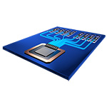
Avicena partners with Lumileds to demonstrate microLED-based LightBundle™ chip-to-chip interconnects with superior energy efficiency and bandwidth density.
SAN DIEGO--(BUSINESS WIRE)--AvicenaTech Corp., a privately held company in Mountain View, CA, is demonstrating its LightBundle™ multi-Tbps chip-to-chip interconnect technology at the Optical Fiber Communications (OFC) Conference in San Diego, CA (https://www.ofcconference.org/en-us/home/exhibition-and-show-floor-programs/).
Interconnects have become the key bottleneck in modern compute and networking systems. Highly variable workloads are driving the evolution of densely interconnected, heterogeneous, software-defined clusters of XPUs, hardware accelerators, and high-performance shared memory. Exploding Artificial Intelligence (AI)/Machine Learning (ML) and High-Performance Computing (HPC) workloads are accelerating the need for interconnects with ultra-low power consumption, ultra-high bandwidth density, and low latency.
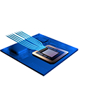
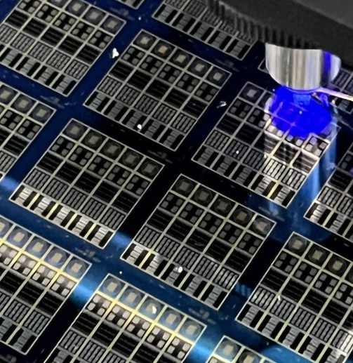
“We have already demonstrated LightBundle™ links at less than 2pJ/bit using our LightBundle™ technology,” says Bardia Pezeshki, founder and CEO of Avicena, “and will soon demonstrate sub-1pJ/bit links.” LightBundle™ is based on arrays of innovative GaN micro-emitters that leverage the microLED display ecosystem and can be integrated onto high performance CMOS ICs. Avicena is working with Lumileds, one of the world’s top GaN LED innovators, to rapidly ramp production of highly optimized microLED arrays.
“Avicena’s demonstration of record low power consumption with its LightBundle™ interconnect technology is proof of the advances Lumileds has made in microLEDs,” says Willem Sillevis-Smitt, Head of Marketing at Lumileds. “We are looking forward to enabling vastly lower power in data center interconnects.”
About the Technology
Today’s high-performance ICs use SerDes-based electrical links to achieve adequate IO density. However, the power consumption and bandwidth density of these electrical links degrade quickly with length. Conventional optical communications technologies developed for networking applications have been impractical for inter-processor and processor-memory interconnects due to their low bandwidth density, high power consumption, high cost, and inability to be co-packaged with hot ASICs.
“All of this is now changing,” says Bardia Pezeshki. “We have developed ultra-low power, high-density optical transceivers based on microLEDs. These innovative devices leverage recent display industry advances and would have been impractical just a few years ago. Our optimized links support up to 10Gbps per lane over -40°C to +125°C temperature with excellent reliability. A LightBundle interconnect uses hundreds of parallel optical lanes connecting microLED arrays to CMOS-compatible PD arrays over multi-core fiber to create low-cost multi-Tbps interconnects with a 10 meter reach.”
The parallel nature of LightBundle™ is well matched to parallel chiplet interfaces like UCIe, OpenHBI, and BoW, and can also be used to extend the reach of compute interconnects like PCIe/CXL, HBM/DDR/GDDR memory links, as well as various inter-processor interconnects like NVLink with low power and low latency.
Avicena at OFC 2022:
In addition to show casing the LightBundle™ technology at the OFC exhibits (booth #3351) Avicena will also present at the following events:
Session Time: March 8, 2022 from 2 PM to 4 PM PST
Session Title: What are the Parallelization Technologies for Cost and Energy Efficient 1.6Tb Links?
Dr. Bardia Pezeshki will participate on the panel and give an invited talk on:
Dense Spatially Multiplexed-Lanes for Short Reach Optics Using Incoherent Optical Sources
Session Time: March 9, 2022 from 8 AM to 10 AM PST
Session Title: Packaging and Co-packaged Optics
Dr. Bardia Pezeshki will give an invited talk on:
MicroLED array-based optical links using an imaging fiber for chip-to-chip communications
Session Time: March 9, 2022 from noon to 2 PM PST
Session Title: OCP Panel: Beyond silicon photonics – New technologies for pluggable and co-packaged optics?
Dr. Chris Pfistner will participate in the OCP Luncheon and Panel followed by a Round Table Discussion
Ultra-low-energy microLED-based optical interconnects for chip-to-chip communications
About Avicena
Avicena Tech Corp. is a privately held company located in Mountain View, CA, specializing in the development of next-generation chip-to-chip interconnects that are more power efficient, offer higher bandwidth density and support longer reach than any current optical or electrical solution. Avicena’s technology is a key building block in the evolution of new computer architectures that will reduce the energy impact on our planet.
Contacts
Avicena Media Contact:
Sama Pourmojib
email: sama@avicena.tech