Samsung Receives Its First Global Carbon Footprint Certification for Logic Chips
Samsung Receives Its First Global Carbon Footprint Certification for Logic Chips
Four high-performance, low-power chips obtain Carbon Trust’s CO2 Measured product carbon footprint label, paving way for carbon reduction
Samsung’s ‘eco-friendly’ fabrication efforts expand further to a wider range of products
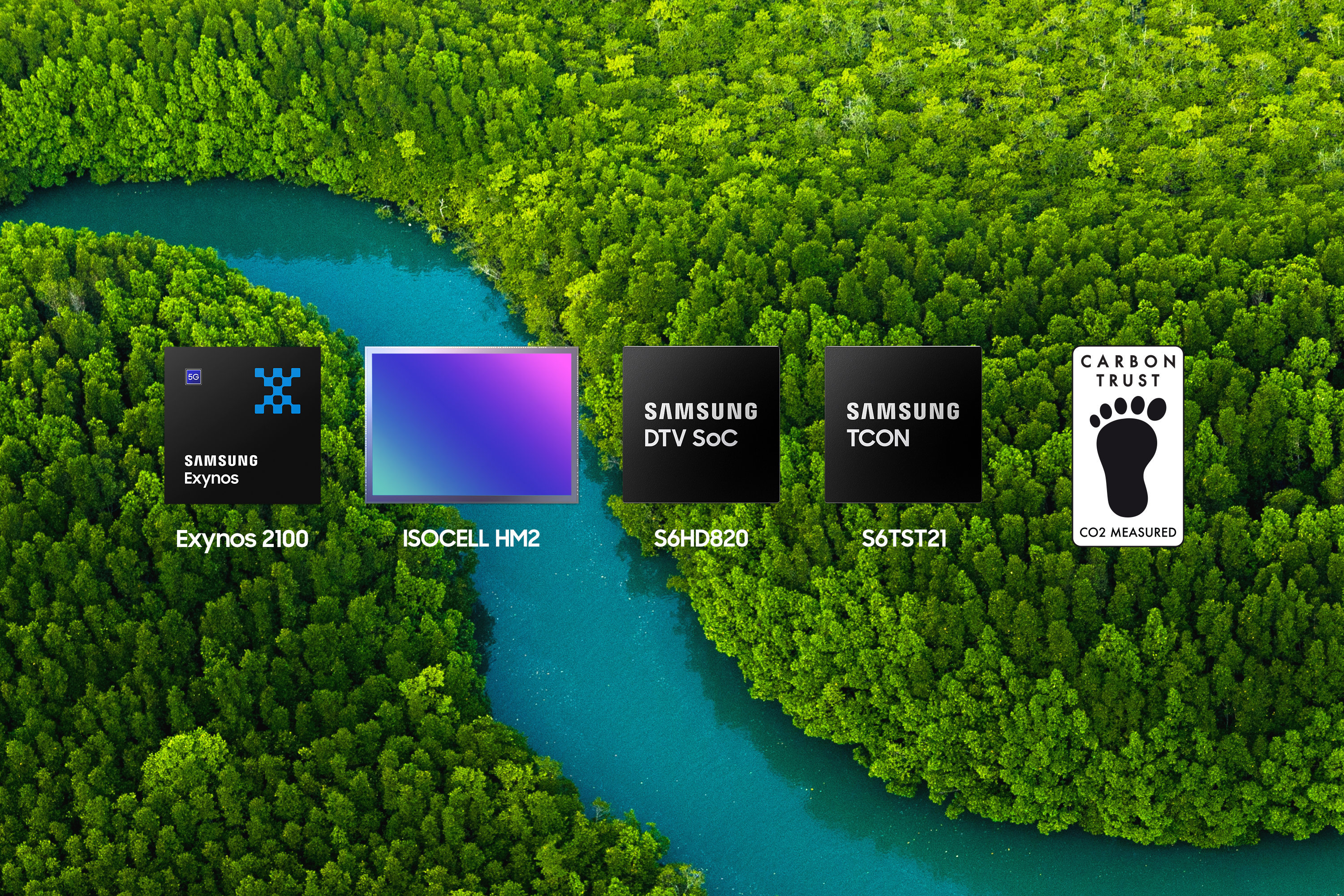
SEOUL, South Korea--(BUSINESS WIRE)--Samsung Electronics Co., Ltd., a world leader in advanced semiconductor technology, today announced that four of its System LSI products received product carbon footprint label certification from the Carbon Trust, the first of Samsung’s logic chips to do so.
Having received the semiconductor industry’s first carbon footprint accreditation for memory chips from the Carbon Trust in 2019, Samsung has now broadened its ESG (Environmental, Social, and Governance) spectrum with this global recognition of ‘eco-friendly’ logic chips. Samsung also grabbed the industry’s first triple Carbon Trust Standard for Carbon, Water and Waste in June 2021.
The Carbon Trust is an independent and expert partner of organizations around the world that advises businesses on their opportunities in a sustainable, low carbon world. The Carbon Trust also measures and certifies the environmental footprint of organizations, supply chains and products.
Of the various certification categories of the Carbon Trust, Samsung’s System LSI products received the CO2 Measured product carbon footprint label. The label certifies the chip’s carbon footprint, which informs consumers of the impact that the product and its manufacturing process have on the environment.
Receiving the CO2 Measured label is a critical first step for carbon reduction, since it verifies the current carbon emissions of the product with globally recognized specifications (PAS 2050), which Samsung can use as a benchmark to measure future carbon reductions.
Correctly measuring the carbon footprint of a product requires extensive effort and time. It involves calculating the amount of carbon emitted from fabricating raw subsidiary materials and transporting the product, as well as the carbon emission from using electricity, water, and gas. The hundreds of fabrication processes needed to make a semiconductor chip adds to the complication.
“We’re pleased to have worked with Samsung on this step in its sustainability journey,” said Hugh Jones, managing director at the Carbon Trust Advisory. “The Carbon Trust’s Carbon Measured certification is a clear and credible indicator for consumers that the carbon footprint of these products have been independently verified, as well as a baseline for Samsung to compare against as they work towards reducing their emissions in the future.”
The four products to receive certification include a variety of Samsung’s System LSI chips, from mobile processors to image sensors. The Exynos 2100, one of the four products to receive certification, is a high-performance mobile processor built with the most advanced 5-nanometer (nm) extreme ultra-violet (EUV) process node. The 0.7-micrometer (μm)-pixel image sensor ISOCELL HM2, DTV SoC (S6HD820), and TCON (S6TST21) also received certification by the Carbon Trust.
Including the four chips, Samsung has so far received certifications for fourteen of its semiconductor products from the Carbon Trust.
“We are thrilled to be globally acknowledged for our eco-friendly efforts,” said Seong-dai Jang, senior vice president and head of DS Corporate Sustainability Management Office at Samsung Electronics. “We will continue to fulfill our carbon reduction goals and expand our efforts to a wider range of eco-friendly, high-performance products to meet the global standards for a sustainable future.”
Exynos 2100
Based on 5nm EUV process technology, the Exynos 2100 is Samsung’s first 5G-integrated flagship mobile processor for premium mobile devices. The Exynos 2100 performs up to 26-trillion-operations-per-second (TOPS) with more than twice the power efficiency than the previous generation.
ISOCELL HM2
The ISOCELL HM2 is a 0.7μm-pixel image sensor that opened up the market for ultra-high resolutions. The 108MP-sensor is around 15 percent smaller than the 0.8μm-based predecessors, and reduces the height of the camera module by 10 percent, while featuring faster autofocus, nine-pixel binning and 3x lossless zoom.
DTV SoC (S6HD820)
Samsung’s DTV SoC (S6HD820) is an essential component in television as picture quality evolves from 4K to 8K standard. The DTV SoC’s NPU (neural processing unit) allows AI technology to improve picture quality and audio processing.
TCON (S6TST21)
A TCON takes video data from the DTV SoC and converts it according to the demands of the DDI (Display Driver IC). The data transmission speed of the TCON is important when it comes to quickly transmitting high-resolution video data to the DDI. Samsung’s TCON (S6TST21) integrates two 8K 60-hertz (Hz) chips to minimize energy loss.
About Samsung Electronics Co., Ltd.
Samsung inspires the world and shapes the future with transformative ideas and technologies. The company is redefining the worlds of TVs, smartphones, wearable devices, tablets, digital appliances, network systems, and memory, system LSI, foundry and LED solutions. For the latest news, please visit the Samsung Newsroom at http://news.samsung.com.
Contacts
Ujeong Jahnke
Samsung Semiconductor Europe GmbH
Tel. +49(0)89-45578-1000
Email: sseg.comm@samsung.com