Samsung Breaks New Ground with Mass Production of Industry’s Smallest 0.64μm-pixel Mobile Image Sensor
Samsung Breaks New Ground with Mass Production of Industry’s Smallest 0.64μm-pixel Mobile Image Sensor
Samsung’s most versatile image sensor offers 50Mp options for both front and rear-facing cameras
Combined pixel technology advancements reduce chip size while enhancing light sensitivity and phase detection capabilities

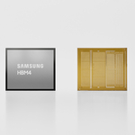
SEOUL, South Korea--(BUSINESS WIRE)--Samsung Electronics Co., Ltd., a world leader in advanced semiconductor technology, today introduced the industry’s first 0.64-micrometer (μm)-pixel image sensor, the 50-megapixel (Mp) Samsung ISOCELL JN1. Equipped with the latest pixel technologies such as enhanced ISOCELL 2.0, Smart-ISO and Double Super PDAF, the JN1 can capture more vivid images on the industry’s smallest 50Mp mobile sensor.
“Samsung’s advanced pixel technologies have once again pushed boundaries with the utmost precision to develop an image sensor with the industry’s smallest pixel size, yet with powerful performance. The new ISOCELL JN1 at 0.64μm will be able to equip tomorrow’s sleekest smartphones with ultra-high resolution mobile photographs,” said Duckhyun Chang, executive vice president of the sensor business at Samsung Electronics. “As we drive our commitment to innovation in pixel technologies, we will continue to bring a wide range of mobile image sensor offerings to the market.”
A new addition to Samsung’s high-resolution image sensor lineup, the JN1 employs ISOCELL 2.0 technology with added enhancements that improve light sensitivity by around 16-percent. For low-light environments, the sensor utilizes Samsung’s four-to-one pixel binning technology, Tetrapixel, which merges four adjacent 0.64μm-pixels into one big 1.28μm-pixel to quadruple light sensitivity for brighter 12.5Mp photographs.
With such advanced technologies all embedded in a small 1/2.76-inch optical format, the ISOCELL JN1 is the most versatile image sensor yet from Samsung. Through close collaboration with ecosystem partners, the JN1 is compatible with existing 1/2.8-inch products, allowing the sensor to be used for front-facing, ultra-wide or telephoto cameras, in addition to standard wide camera options. This means that users can take highly detailed selfies or group pictures in an amazing 50Mp resolution, as well as high-resolution video at up to 4K and high-zoom ratios. The smaller sensor can also reduce the height of the camera module by around 10-percent, minimizing the camera bulge for slimmer and more streamlined designs in next-generation smartphones.
For enhanced dynamic range, the ISOCELL JN1 comes with Smart-ISO, a technology that changes the conversion gain based on the environment’s illumination level. Smart-ISO uses Low ISO mode in bright settings to retain detail in the highlights, and High ISO in low-lit environments to reduce readout noise and generate excellent low-light performance. Using Smart-ISO, the JN1 also offers inter-scene HDR in mixed-light settings for optimum exposure levels derived from two separate readouts, from Low and High ISOs, that are merged to create a final image.
For faster auto-focus, the ISOCELL JN1 integrates improved Double Super PD. The previous Super PD technology used specially designed oval-shaped micro-lenses over two adjacent pixels arranged side by side to detect phases. Double Super PD features twice the density of pixels (1/16) used for phase detection than Super PD (1/32), enabling the same auto-focus performance even in environments with about 60-percent less illumination levels. For smooth crystal-clear videos, the image sensor supports up to 4K resolution video recording at 60 frames-per-second (fps) or full HD at 240fps.
The Samsung ISOCELL JN1 is currently in mass production.
* Editor's Note: Actual performance may vary depending on device and user environment.
* Samsung first announced its ISOCELL technology in 2013, which reduces color crosstalk between pixels by placing a physical barrier, allowing small-sized pixels to achieve higher color fidelity. Based on this technology, Samsung introduced the industry’s first 1.0um-pixel image sensor in 2015 and a 0.9-pixel sensor in 2017. Samsung continues to enhance its pixel isolation methods with ISOCELL Plus and the ISOCELL 2.0 technologies.
###
About Samsung Electronics Co., Ltd.
Samsung inspires the world and shapes the future with transformative ideas and technologies. The company is redefining the worlds of TVs, smartphones, wearable devices, tablets, digital appliances, network systems, and memory, system LSI, foundry and LED solutions. For the latest news, please visit the Samsung Newsroom at http://news.samsung.com.
Contacts
Ujeong Jahnke
Samsung Semiconductor Europe GmbH
Tel. +49(0)89-45578-1000
Email: sseg.comm@samsung.com