Newsroom
Sorted by: Latest
-
TemperPack Becomes a Certified B Corporation™
RICHMOND, Va.--(BUSINESS WIRE)--TemperPack®, the leader in sustainable thermal packaging, has earned certification from the nonprofit B Lab as a B Corporation™, joining a global community of companies held to the highest verified standards of social and environmental performance, accountability, and transparency. The certification spans the entire TemperPack business and marks a defining milestone for a company that has spent a decade displacing legacy plastics with science-driven, sustainable...

-
Bank of New York Mellon UK Regulatory Announcement: FRN Variable Rate Fix
LONDON--(BUSINESS WIRE)-- As Agent Bank, please be advised of the following rate determined on: 4/27/2026 Issue ¦ National Bank of Canada - Series CBL20 GBP 750,000,000 FRN due May 2026 ISIN Number ¦ XS2474786980 ISIN Reference ¦ 247478698 Issue Nomin GBP ¦ 750000000 Period ¦ 2/5/2026 to 5/5/2026 Payment Date 5/5/2026 Number of Days ¦ 89 Rate ¦ 4.74512 Denomination GBP ¦ 1000 ¦ 750000000 ¦ Amount Payable per Denomination ¦ 11.57 ¦ 8677719.45 ¦ Bank of New York R...
-
Innovative L.A. Law Firm J&Y Law Saves 320 Hours of Work Each Week Due to Strategic AI Tech Adoption
LOS ANGELES--(BUSINESS WIRE)--J&Y Law, a California injury law firm based in L.A., transformed by leveraging EvenUp AI tech which is specifically for personal injury law....

-
Law Offices of Frank R. Cruz Encourages LKQ Corporation (LKQ) Shareholders To Inquire About Securities Fraud Class Action
LOS ANGELES--(BUSINESS WIRE)--Law Offices of Frank R. Cruz Encourages LKQ Corporation (LKQ) Shareholders To Inquire About Securities Fraud Class Action....
-
SergeFerrari Group: Assemblée Générale Mixte du 22 avril 2026
SAINT-JEAN-DE-SOUDAIN, France--(BUSINESS WIRE)--Regulatory News: SergeFerrari Group (FR0011950682 - SEFER), l’un des leaders mondiaux dans les toiles composites innovantes, est coté sur Euronext Paris - compartiment C. Conformément aux dispositions de l'article R. 22-10-30 du Code de commerce, nous vous informons du résultat du vote des résolutions présentées à l'assemblée générale mixte des actionnaires de la société SergeFerrari Group du 22 avril 2026. Les actionnaires présents, représentés,...
-
WestJet Flight Attendants Issue Notice of Dispute
Calgary, AB--(BUSINESS WIRE)--Flight Attendants at WestJet, represented by CUPE 8125, have issued a formal notice of dispute following more than seven months of ongoing negotiations that have not produced sufficient progress on key issues. CUPE 8125 represents approximately 4,400 cabin personnel at WestJet mainline. Since serving notice to bargain last September, the union and WestJet have met multiple times each month in an effort to reach a new collective agreement. At the centre of the dispu...
-
SMAIO : Mise à disposition du rapport financier annuel 2025
DALLAS & LYON, France--(BUSINESS WIRE)--Regulatory News: SMAIO (Software, Machines and Adaptative Implants in Orthopaedics – Euronext Growth Paris, Code ISIN : FR0014005I80 / Mnémonique : ALSMA, éligible PEA-PME), une société franco-américaine spécialisée dans la chirurgie rachidienne complexe proposant une solution intégrée pré, intra et postopératoire basée sur un logiciel de planification 3D, des implants adaptatifs et des services associés, annonce aujourd’hui que son rapport financier annu...
-
Perini Management Services, Inc. Awarded the Right to Compete for Task Orders Under $2 Billion USACE Energy Resilience and Conservation Investment Program
FRAMINGHAM, Mass.--(BUSINESS WIRE)--Tutor Perini Corporation (NYSE: TPC) (the “Company”), a leading civil, building and specialty construction company, announced today that its subsidiary, Perini Management Services, Inc. (“PMSI”), has been awarded a construction multiple-award task order contract (“MATOC”) by the U.S. Army Corps of Engineers (“USACE”), Louisville District. The contract provides a shared capacity of $2 billion over 10 years (a three-year base period and seven one-year option pe...

-
Chord Music Partners Prices $500 Million ABS Backed by Diversified Music Catalog
NEW YORK--(BUSINESS WIRE)--Chord Music Partners, a leading global music investment platform managed by Dundee Partners in partnership with Universal Music Group (UMG), the world leader in music-based entertainment, today announced the pricing of $500 million of Series 2026-1 senior notes (the “Notes”), secured by a diversified portfolio of music publishing and recorded music assets. The Notes are expected to be issued by Canon Music Issuer Trust, which is intended to serve as Chord’s long-term...
-
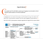
OpenEvidence Collaborates With NCCN to Integrate Canonical Oncology Treatment Algorithms at the Point-of-Care
MIAMI--(BUSINESS WIRE)--OpenEvidence now integrates National Comprehensive Cancer Network® (NCCN®) Clinical Practice Guidelines in Oncology (NCCN Guidelines®) directly in answers, grounding responses in the pinnacle reference resource defining and advancing care in oncology. OpenEvidence’s collaboration with NCCN marks the beginning of a series of focused oncology-related updates to the platform—in conjunction with leading experts in oncology—to help clinicians give the best possible care to pa...