Samsung Electronics Begins Mass Production of 8th-Gen Vertical NAND with Industry’s Highest Bit Density
Samsung Electronics Begins Mass Production of 8th-Gen Vertical NAND with Industry’s Highest Bit Density
Samsung’s eighth-generation V-NAND features both the industry’s highest storage capacity and highest bit density to enable expanded storage space in next-generation servers
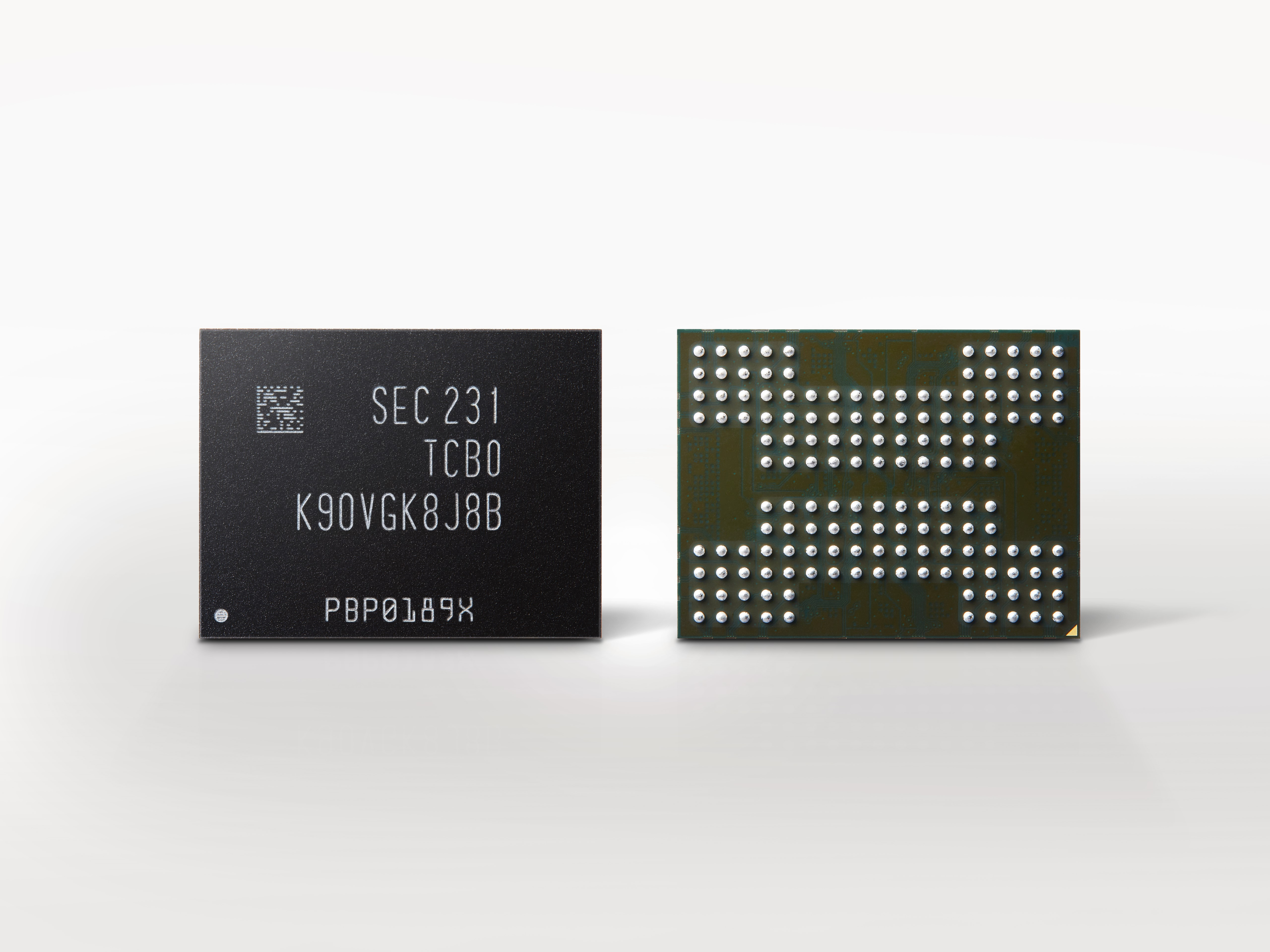
SEOUL, South Korea--(BUSINESS WIRE)--Samsung Electronics Co., Ltd., the world leader in advanced memory technology, as promised at Flash Memory Summit 2022 and Samsung Memory Tech Day 2022, announced today that it has begun mass producing a 1-terabit (Tb) triple-level cell (TLC) eighth-generation Vertical NAND (V-NAND) with the industry’s highest bit density. At 1Tb, the new V-NAND also features the highest storage capacity to date, enabling larger storage space in next-generation enterprise server systems worldwide.
"As market demand for denser, greater-capacity storage pushes for higher V-NAND layer counts, Samsung has adopted its advanced 3D scaling technology to reduce surface area and height, while avoiding the cell-to-cell interference that normally occurs with scaling down," said SungHoi Hur, Executive Vice President of Flash Product & Technology at Samsung Electronics. "Our eighth-generation V-NAND will help meet rapidly growing market demand and better position us to deliver more differentiated products and solutions, which will be at the very foundation of future storage innovations."
Samsung was able to attain the industry’s highest bit density by significantly enhancing the bit productivity per wafer. Based on the Toggle DDR 5.0 interface* — the latest NAND flash standard — Samsung’s eighth-generation V-NAND features an input and output (I/O) speed of up to 2.4 gigabits per second (Gbps), a 1.2X boost over the previous generation. This will enable the new V-NAND to accommodate the performance requirements of PCIe 4.0, and later, PCIe 5.0.
The eighth-generation V-NAND is expected to serve as the cornerstone for storage configurations that help expand the storage capacity in next-generation enterprise servers, while extending its use into the automotive market where reliability is especially critical.
* Editor’s note: Toggle DDR interface generations — 1.0 (133Mbps), 2.0 (400Mbps), 3.0 (800Mbps), 4.0 (1,200Mbps), 5.0 (2,400Mbps)
###
About Samsung Electronics Co., Ltd.
Samsung inspires the world and shapes the future with transformative ideas and technologies. The company is redefining the worlds of TVs, smartphones, wearable devices, tablets, digital appliances, network systems, and memory, system LSI, foundry and LED solutions. For the latest news, please visit the Samsung Newsroom at news.samsung.com.
Contacts
Ujeong Jahnke
Samsung Semiconductor Europe GmbH
Tel. +49(0)89-45578-1000
Email: sseg.comm@samsung.com