Newsroom
Sorted by: Latest
-
Swedish Court Reschedules Publication of Judgment in PriceRunner Vs Google Antitrust Case
STOCKHOLM--(BUSINESS WIRE)--Klarna Group plc (NYSE: KLAR) wishes to update investors that the Patent and Market Court in Stockholm, Sweden (Patent- och marknadsdomstolen) has postponed publication of its judgment in the antitrust damages proceedings brought by PriceRunner, a Klarna subsidiary, against Google. The Court has rescheduled publication of its judgment from 10 June to 26 June, 2026 at 11:00 CET. Important Notice The outcome of the proceedings is inherently uncertain. No assurance can...

-
OutSystems Recognizes Leaders Driving Real AI Impact at the 2026 ONE Conference
AMSTERDAM--(BUSINESS WIRE)--OutSystems, a leading Agentic Systems platform, today announced the winners of its 2026 Innovation Awards, the industry benchmark for showcasing how customers are leveraging AI to create real-world impact. Leading organizations across retail, manufacturing, energy, distribution and other sectors were recognized for moving beyond AI experimentation to deliver high-impact, mission-critical agents, agentic systems and applications that advance their business and society...

-
Everest Funeral Concierge Partners With WTW
LONDON--(BUSINESS WIRE)--Everest Funeral Concierge UK has partnered with WTW to make Everest’s funeral planning and independent advocacy support available to employers who are looking to help support employees and their families before and after bereavements. The partnership marks the first time Everest’s funeral concierge service has been available via a benefits broker in the UK. Everest’s expert advisers are available by telephone 24/7. And with 99% of calls answered within 30 seconds, they...

-
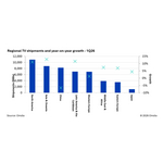
Omdia: TV Shipments Increase 6% in 1Q26 as 2026 World Cup Inventory Build-Up Begins
LONDON--(BUSINESS WIRE)--Global TV shipments increased 6% year-on-year (YoY) to 50.3 million units in 1Q26, as retailers increased inventory ahead of the upcoming 2026 World Cup, according to data from Omdia’s latest TV Sets (Emerging Technologies) Market Tracker: History – 1Q26. All regions grew YoY except for Mainland China, which continues to face weak local demand following domestic stimulus measures in 2025. Developing economies and North America propel global growth The two fastest growin...
-
Natixis Syndicate UK Regulatory Announcement: PRE-STABILISATION ANNOUNCEMENT
LONDON--(BUSINESS WIRE)-- PRE-STABILISATION ANNOUNCEMENT Date: 3 June 2026 Not for distribution, directly or indirectly, in or into the United States or any jurisdiction in which such distribution would be unlawful. Coöperatieve Rabobank U.A. Pre-stabilisation Period Announcement Natixis (contact: Christopher Agathangelou; telephone: 0158550814) hereby gives notice, as Stabilisation Coordinator, that the Stabilisation Manager(s) named below may stabilise the offer of the following securities i...
-
Live Story si espande in Europa, in risposta alla crescente domanda di esperienze digitali no-code
MILANO--(BUSINESS WIRE)--Live Story, Frontend Creative Platform no-code, avvia il proprio percorso di espansione internazionale con un focus strategico su Regno Unito, Irlanda e Paesi Nordici. Una crescita che arriva dopo il forte sviluppo in Italia e Svizzera, dove l’azienda ha raddoppiato il proprio ARR (fatturato ricorrente annuale) nel primo semestre dell’anno rispetto alla fine del 2025. La piattaforma permette ai brand di progettare, gestire e pubblicare esperienze digitali a livelllo ent...

-
Live Story Expands Into Europe’s Most Innovation-Driven Markets Amid Growing Demand for Agile Digital Experiences
MILAN--(BUSINESS WIRE)--Top digital brands move faster than dev cycles. This is where Live Story comes in: a no-code frontend creative platform expanding across Europe....

-
Broadvoice Launches GoEngage and AI Analyst, Bringing Voice AI and Conversational Insights to GoContact
LOS ANGELES--(BUSINESS WIRE)--Broadvoice, a leader in AI-powered customer experience solutions, today announced GoEngage and AI Analyst, two new AI capabilities for GoContact. GoEngage automates inbound voice interactions with a natural, human-like cadence. AI Analyst gives contact center leaders instant answers to operational questions without waiting for reports or dashboards. Together, they mark a major milestone in Broadvoice’s AI strategy and the next stage in its unified brand evolution....

-
Purdys Chocolatier Marks Its Next Chapter of Canadian Growth with Maritimes Expansion
VANCOUVER, British Columbia--(BUSINESS WIRE)--Purdys Chocolatier is expanding into the Maritimes, bringing its rich Canadian heritage from the West Coast to the East Coast, and marking a new chapter in its Canadian history. This September, the beloved Canadian chocolatier, founded in 1907, will open four locations in shopping malls across Nova Scotia and New Brunswick. This milestone adds two new provinces to the brand’s growing national footprint, and Purdys Chocolatier is honoured to bring 11...

-
Veth Propulsion by Twin Disc onthult op Maritime Industry nieuwe generatie voortstuwingstechnologie: Streamline-CRP™
Papendrecht, Nederland--(BUSINESS WIRE)--Veth Propulsion by Twin Disc, wereldwijd leverancier van voortstuwings- en manoeuvreeroplossingen voor de maritieme sector, heeft op 2 juni tijdens Maritime Industry in Gorinchem een nieuwe toevoeging aan haar portfolio gepresenteerd. Bezoekers van de beurs kregen daar als eersten de mogelijkheid om kennis te maken met deze nieuwste innovatie. Het nieuwe product, Streamline-CRP™, betekent een belangrijke volgende stap in de ontwikkeling van contra-rotere...