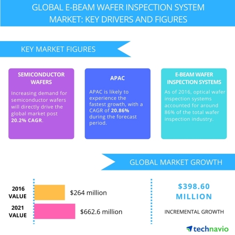
LONDON--(BUSINESS WIRE)--Technavio analysts forecast the global e-beam wafer inspection system market to grow at a CAGR of over 20% during the forecast period, according to their latest report.
The research study covers the present scenario and growth prospects of the global e-beam wafer inspection system market for 2017-2021. To calculate the market size, the report covers the shipment of e-beam wafer inspection equipment worldwide.
Geographically, APAC is the market leader, having a total share of 74.12% by revenue in 2016. One of the important reasons for this dominance is the presence of semiconductor foundries like TSMC, SMIC, and UMC in the region. These foundries manufacture ICs based on the designs provided by fabless semiconductor companies. APAC was followed by the Americas with a share of 18.56% and EMEA with a share of 7.32% in 2016.
There is a high growth potential for this market because of the increase in adoption of these products by semi-conductor manufacturers to ensure high-quality of their products. With a demand for the best quality products, there will be an increased adoption of these systems through the forecast period. ASML is one of the key vendors in this market space, taking several strategic initiatives to strengthen its customer base in the semiconductor sector. The company has received a USD 1.4 billion contract to develop tools for making smaller, more cost-effective chips.
Request a sample report: http://www.technavio.com/request-a-sample?report=55361
Technavio’s sample reports are free of charge and contain multiple sections of the report including the market size and forecast, drivers, challenges, trends, and more.
Technavio analysts highlight the following three factors that are contributing to the growth of the global e-beam wafer inspection system market:
- Increasing demand for semiconductor wafers
- Increasing complexity of semiconductor wafer designs
- Increase in the use for R&D purposes
Increasing demand for semiconductor wafers
“There has been an increase in the adoption of communication devices and consumer electronic equipment such as smartphones, tablets, wearable electronics, liquid crystal displays, and light emitting diodes. These devices utilize high quality semiconductors, like silicone-based wafer, which is indirectly creating a demand for e-beam wafer inspection systems, which play a mojor role in integrated circuits,” says Sunil Kumar Singh, one of the lead analysts at Technavio for semiconductor equipment research.
The increasing demand for semiconductor wafers, which will push for investments from semiconductor foundries to boost their production capacities. Additionally, vendors are focusing on manufacturing miniaturized personal electronics that consume less power. These miniaturized products not only aid in lowering IC power consumption, but also in reducing the size of semiconductor wafers. Therefore, the use of advanced e-beam wafer inspection equipment will increase with the increase in the number of miniaturized wafers.
Increasing complexity of semiconductor wafer designs
With consumers demanding more functionality in electronic devices, the manufacturing of semiconductor wafers is becoming more complex. This has also led to the development of 3D ICs, which are compact, consumes less power, and are more efficient. This advanced technology increases the possibility of defects in wafers, making wafer inspection systems more essential. To manufacture these complex designs, foundries will invest heavily in manufacturing equipment, fab equipment, and assembly and test equipment, to develop advanced production systems, which will bring in significant revenue to the market.
The high circuit densities of modern integrated circuits (ICs) have resulted in the reduction in the cost of their procurement, while their functionalities have increased. With this trend, manufacturers are not limited by the ICs and can experiment with different shapes and sizes of the devices. These new devices will keep the demand for e-beam wafer inspection systems endless, thus creating a constant revenue stream.
Increase in the use for R&D purposes
With increased technical developments in electronic and semiconductor devices, wafer manufacturers are investing heavily to meet the growing demand of the consumers. Constant changes in technology is causing vendors in the e-beam wafer inspection systems to invest heavily in research and development (R&D), to better equip their systems with 3nm resolution capabilities.
"This will have a moderately high impact on semiconductor foundries as e-beam wafer inspection systems works with a very high level of magnification. Furthermore, the charge variation defects can only be inspected using the e-beam system, thereby providing the R&D staff with better information about the smallest of defects,” says Sunil.
Browse Related Reports:
- Global Semiconductor Inspection Systems Market 2016-2020
- Global Optical Patterned Wafer Inspection Equipment Market 2015-2019
- Global Semiconductor Wafer Cleaning Systems Market 2015-2019
Become a Technavio Insights member and access all three of these reports for a fraction of their original cost. As a Technavio Insights member, you will have immediate access to new reports as they’re published in addition to all 6,000+ existing reports covering segments like embedded systems, human machine interface, and sensors. This subscription nets you thousands in savings, while staying connected to Technavio’s constant transforming research library, helping you make informed business decisions more efficiently.
About Technavio
Technavio is a leading global technology research and advisory company. The company develops over 2000 pieces of research every year, covering more than 500 technologies across 80 countries. Technavio has about 300 analysts globally who specialize in customized consulting and business research assignments across the latest leading edge technologies.
Technavio analysts employ primary as well as secondary research techniques to ascertain the size and vendor landscape in a range of markets. Analysts obtain information using a combination of bottom-up and top-down approaches, besides using in-house market modeling tools and proprietary databases. They corroborate this data with the data obtained from various market participants and stakeholders across the value chain, including vendors, service providers, distributors, re-sellers, and end-users.
If you are interested in more information, please contact our media team at media@technavio.com.


