

Newsroom
Sorted by: Latest
-
ImmunityBio, Inc. Sued for Securities Law Violations - Contact the DJS Law Group to Discuss Your Rights – IBRX
LOS ANGELES--(BUSINESS WIRE)--ImmunityBio, Inc. Sued for Securities Law Violations - Contact the DJS Law Group to Discuss Your Rights – IBRX...
-
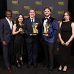
45th College Television Awards Winners Announced by Television Academy Foundation
LOS ANGELES--(BUSINESS WIRE)--The Television Academy Foundation announced the winners of the 45th College Television Awards, which recognize and reward excellence in student-produced programs from colleges nationwide, tonight at a star-studded awards presentation at the Saban Media Center in North Hollywood, California. The 2026 winners were presented awards by top television stars including Samuel Arnold (Emily in Paris), Rhenzy Feliz (The Penguin), Ashby Florence (TikTok influencer), Ezra Fre...
-
SMCI Investors Have Opportunity to Lead Super Micro Computer, Inc. Securities Fraud Lawsuit with the Schall Law Firm
LOS ANGELES--(BUSINESS WIRE)--SMCI Investors Have Opportunity to Lead Super Micro Computer, Inc. Securities Fraud Lawsuit with the Schall Law Firm...
-
IBRX Investors Have Opportunity to Lead ImmunityBio, Inc. Securities Fraud Lawsuit with the Schall Law Firm
LOS ANGELES--(BUSINESS WIRE)--IBRX Investors Have Opportunity to Lead ImmunityBio, Inc. Securities Fraud Lawsuit with the Schall Law Firm...
-
WMK Investors Have Opportunity to Join Weis Markets, Inc. Fraud Investigation with the Schall Law Firm
LOS ANGELES--(BUSINESS WIRE)--WMK Investors Have Opportunity to Join Weis Markets, Inc. Fraud Investigation with the Schall Law Firm...
-
EVTL Investors Have Opportunity to Join Vertical Aerospace Ltd. Fraud Investigation with the Schall Law Firm
LOS ANGELES--(BUSINESS WIRE)--EVTL Investors Have Opportunity to Join Vertical Aerospace Ltd. Fraud Investigation with the Schall Law Firm...
-
SAN Investors Have Opportunity to Join Banco Santander, S.A. Fraud Investigation with the Schall Law Firm
LOS ANGELES--(BUSINESS WIRE)--SAN Investors Have Opportunity to Join Banco Santander, S.A. Fraud Investigation with the Schall Law Firm...
-
BW Investors Have Opportunity to Join Babcock & Wilcox Enterprises, Inc. Fraud Investigation with the Schall Law Firm
LOS ANGELES--(BUSINESS WIRE)--BW Investors Have Opportunity to Join Babcock & Wilcox Enterprises, Inc. Fraud Investigation with the Schall Law Firm...
-
Kardigan Announces Positive Phase 2 Data for Tonlamarsen in Patients with Uncontrolled Hypertension Presented as Late-Breaker at ACC.26 and Simultaneously Published in JACC
SOUTH SAN FRANCISCO, Calif., & PRINCETON, N.J.--(BUSINESS WIRE)--Kardigan announced results from KARDINAL, a Phase 2 clinical trial evaluating the effects of tonlamarsen in patients with uncontrolled hypertension....
-
Debevoise Secures Second Circuit Affirmance of Dismissal of $16 billion Claim Against YPF S.A.
NEW YORK--(BUSINESS WIRE)--Debevoise & Plimpton LLP has secured affirmance from the U.S. Court of Appeals for the Second Circuit of its 2023 summary judgment win on behalf of YPF S.A., the largest energy producer in the Republic of Argentina – defeating claims for more than $16 billion in damages and interest. This is a landmark win for YPF, affirming the dismissal of a case that has been pending in S.D.N.Y since 2015. The Second Circuit fully affirmed the District Court’s holding that YPF...