Newsroom
Sorted by: Latest
-
Neuer Cloudflare-Bericht warnt vor einer „technischen Glasdecke“, die das Wachstum der KI hemmt und die Cybersicherheit schwächt
SAN FRANCISCO--(BUSINESS WIRE)--Cloudflare, Inc. (NYSE: NET), das führende Unternehmen für Konnektivitäts-Cloud-Lösungen, hat heute seinen ersten 2026 App Innovation Report veröffentlicht. Die Ergebnisse des Berichts zeigen eine deutliche Kluft: Unternehmen, die der Modernisierung von Anwendungen Priorität einräumen – d. h. die ihre Tech-Stacks aktualisieren, um sich von veralteten Systemen zu lösen –, können KI erfolgreich einsetzen und ihre Sicherheit gewährleisten, während diejenigen, die mi...
-
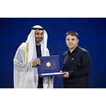
Bodrum Anatolian High School Wins the 2026 Zayed Sustainability Prize in the Global High Schools – Europe & Central Asia Category
ABU DHABI, United Arab Emirates--(BUSINESS WIRE)--Bodrum Anatolian High School Wins the 2026 Zayed Sustainability Prize in the Global High Schools – Europe & Central Asia Category...
-
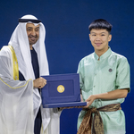
Ruamrudee International School Wins the 2026 Zayed Sustainability Prize in the Global High Schools – East Asia & Pacific Category
ABU DHABI, United Arab Emirates--(BUSINESS WIRE)--Ruamrudee International School Wins the 2026 Zayed Sustainability Prize in the Global High Schools – East Asia & Pacific Category...
-
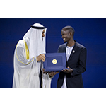
Kyanja High School Wins the 2026 Zayed Sustainability Prize in the Global High Schools – Sub-Saharan Africa Category
ABU DHABI, United Arab Emirates--(BUSINESS WIRE)--Kyanja High School Wins the 2026 Zayed Sustainability Prize in the Global High Schools – Sub-Saharan Africa Category...
-
Mitsubishi Electric to Strengthen Global Human Resources Allocation and Development with Talent Mobility and G-OJT Systems
TOKYO--(BUSINESS WIRE)--Mitsubishi Electric Corporation (TOKYO: 6503) announced today that it will launch the Talent Mobility System to match employees with jobs in the company’s global group in order to develop, mobilize and engage top talent. It will also revise the Global- On the Job Training (G-OJT) System to provide young employees with deeper overseas work experiences compared to those of conventional overseas temporary-training programs. Mitsubishi Electric, which employs approximately 1...
-
Build up Nepal Wins the 2026 Zayed Sustainability Prize in the Climate Action Category
ABU DHABI, United Arab Emirates--(BUSINESS WIRE)--Build up Nepal Wins the 2026 Zayed Sustainability Prize in the Climate Action Category...

-
Corcept Therapeutics Incorporated Investigated on Behalf of Investors - Contact the DJS Law Group to Discuss Your Rights – CORT
LOS ANGELES--(BUSINESS WIRE)--Corcept Therapeutics Incorporated Investigated on Behalf of Investors - Contact the DJS Law Group to Discuss Your Rights – CORT...
-
ORCL Investors Have Opportunity to Join Oracle Corporation Fraud Investigation with the Schall Law Firm
LOS ANGELES--(BUSINESS WIRE)--ORCL Investors Have Opportunity to Join Oracle Corporation Fraud Investigation with the Schall Law Firm...
-
FPT Recognized in Everest Group Banking IT Services PEAK Matrix® Assessment 2025
HANOI, Vietnam--(BUSINESS WIRE)--Global IT services provider FPT has been positioned as a Major Contender in the Everest Group Banking IT Services PEAK Matrix® Assessment 2025, marking its first appearance in this industry benchmark. The research evaluates 41 providers for the banking IT services. Providers are grouped into Leaders, Major Contenders, Aspirants, and Star Performers based on their ability to support modernization, adopt agentic AI in a responsible and scalable way, and help banks...

-
Riassunto: Alpaca raccoglie 150 milioni di dollari a una valutazione di 1,15 miliardi di dollari per costruire lo standard globale delle infrastrutture di mediazione
SAN MATEO, Calif.--(BUSINESS WIRE)--Alpaca, un leader globale nelle infrastrutture di mediazione, le cui API alimentano aziende partner come Kraken, SBI Securities e Dime!, oggi hanno annunciato di aver raccolto 150 milioni di dollari in un round di finanziamento di serie D condotto da Drive Capital che valuta la società a 1,15 miliardi di dollari. Il cofondatore e socio di Drive Capital, Chris Olsen, si unirà al CdA di Alpaca come previsto dall'investimento. La società si è inoltre assicurata...