

Newsroom
Sorted by: Latest
-
UK Debt Management Office UK Regulatory Announcement: Issue of Debt
LONDON--(BUSINESS WIRE)-- DMO-TAS041/3681/003 The Minster Building21 Mincing LaneLondonEC3R 7AG T 020 7862 6500F 020 7862 6509www.dmo.gov.uk A075\26 11 June 2026 PRESS NOTICE RESULT OF THE SALE BY AUCTION OF £5000 MILLION OF 4% TREASURY GILT 2029The United Kingdom Debt Management Office ("DMO") announces that the auction of £5,000 million of 4% Treasury Gilt 2029 (ISIN Code: GB00BVP99566) has been allocated as follows:(Note: all prices in this notice are quoted in pounds...
-
Conférence sur l’Internet de l’énergie de Chine 2026 lancée à Qingdao, mettant en avant la transformation numérique et verte
QINGDAO, Chine--(BUSINESS WIRE)--La Conférence sur l’Internet de l’énergie de Chine 2026 s’est ouverte le 6 juin à Qingdao, dans la province du Shandong, à l’est de la Chine. Elle a réuni plus de 1 000 responsables gouvernementaux, experts du secteur, universitaires ainsi que des représentants d’entreprises énergétiques, d’instituts de recherche et du secteur financier, afin d’explorer des voies de transformation énergétique de haute qualité pour la Chine. La conférence de deux jours est organi...

-
China Energy Internet Conference 2026 Kicks Off in Qingdao, Highlighting Digital and Green Transformation
QINGDAO, China--(BUSINESS WIRE)--The 2026 China Energy Internet Conference kicked off on June 6 in Qingdao, East China's Shandong Province, gathering over 1,000 government officials, industry elites, scholars and representatives from energy firms, research institutions and financial sectors to explore high-quality pathways for China's energy transformation. The two-day event is hosted by Tsinghua University and organized by its Energy Internet Research Institute. Co-organizers include the unive...
-
Faire celebra cinco años de crecimiento fuera de Norteamérica: más de 100 000 minoristas, 50 000 marcas y más de una de cada cuatro marcas que ya venden en el extranjero
LONDRES--(BUSINESS WIRE)--Cinco años después de su lanzamiento fuera de Norteamérica, la comunidad de Faire, compuesta por más de 100 000 comercios y 50 000 marcas repartidas por más de 30 países de Europa, Australia y Nueva Zelanda, pone de manifiesto que el sector minorista está innovando y prosperando, mucho más allá de las grandes ciudades. "Han sido cinco años extraordinarios para Faire a nivel internacional, y las oportunidades que se nos presentan nunca han estado tan claras", afirmó Oli...

-
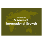
Faire Marks Five Years of Growth Outside North America: Over 100,000 Retailers, 50,000 Brands, and More Than One in Four Brands Now Selling Across Borders
LONDON--(BUSINESS WIRE)--Five years after launching outside North America, Faire’s community of more than 100,000 retailers and 50,000 brands across 30+ countries in Europe, Australia, and New Zealand shows a retail sector that is innovating and thriving, well beyond the big cities. "It has been a phenomenal five years for Faire internationally, and the opportunity ahead has never been clearer,” said Olivier Buffon, VP and Head of International at Faire. “Europe represents a retail market compa...

-
Faire célèbre cinq années de croissance hors Amérique du Nord : plus de 100 000 détaillants, 50 000 marques, avec plus d’une marque sur quatre qui effectuent désormais des ventes transfrontalières
LONDRES--(BUSINESS WIRE)--Cinq ans après son lancement en dehors de l'Amérique du Nord, la communauté Faire, qui compte plus de 100 000 détaillants et 50 000 marques répartis dans plus de 30 pays d'Europe, d'Australie et de Nouvelle-Zélande, témoigne d'un secteur du commerce de détail innovant et en plein essor, même très loin des grands centres urbains. « Faire, qui a vécu une période exceptionnelle à l'international pendant les cinq dernières années, voit se dessiner des perspectives d'avenir...

-
Faire annuncia cinque anni di crescita fuori del Nordamerica: oltre 100.000 commercianti al dettaglio, 50.000 marchi e più di un marchio su quattro che ora vende all'estero
LONDRA--(BUSINESS WIRE)--Cinque anni dopo il lancio al di fuori del Nordamerica, la comunità di Faire di oltre 100.000 commercianti al dettaglio e 50.000 marchi in più di 30 Paesi in Europa, Australia e Nuova Zelanda mostra un settore retail innovativo e florido, ben oltre le grandi città. "Sono stati cinque anni fenomenali per Faire a livello internazionale, con prospettive di opportunità mai così chiare”, ha dichiarato Olivier Buffon, VP e Responsabile dei rapporti internazionali di Faire. “L...

-
Faire blickt auf fünf Jahre Wachstum außerhalb Nordamerikas zurück: Über 100.000 Einzelhändler, 50.000 Marken und mehr als jede vierte Marke verkauft mittlerweile grenzüberschreitend
LONDON--(BUSINESS WIRE)--Fünf Jahre nach dem Start außerhalb Nordamerikas zeugt die Faire-Community mit mehr als 100.000 Einzelhändlern und 50.000 Marken in über 30 Ländern in Europa, Australien und Neuseeland von einem Einzelhandelssektor, der innovativ ist und floriert – und zwar weit über die großen Städte hinaus. „Für Faire waren es international fünf phänomenale Jahre, und die vor uns liegenden Chancen waren noch nie so deutlich“, sagte Olivier Buffon, VP und Head of International bei Fair...

-
Faire markeert vijf jaar groei buiten Noord-Amerika: meer dan 100.000 retailers, 50.000 merken en meer dan een op vier merken die nu buiten de landsgrenzen worden verkocht
LONDEN--(BUSINESS WIRE)--Vijf jaar na de lancering buiten Noord-Amerika laat Faires gemeenschap van meer dan 100.000 retailers en 50.000 merken in meer dan 30 landen in Europa, Australië en Nieuw-Zeeland een retailsector zijn die innoveert en floreert, ver buiten de grote steden. "Voor Faire waren het internationaal fenomenale vijf jaren, en de opportuniteit die voor ons ligt was nog nooit zo duidelijk,” verklaart Olivier Buffon, VP en Head of International van Faire. “Europa vormt een retailma...
-
EoS Fitness Plants its Flag in the Alamo City, Expanding its Texas Footprint to San Antonio
DALLAS--(BUSINESS WIRE)--High Value. Low Price.® (HVLP) Gym Chain Debuts in One of the Country’s Fastest-Growing Cities....