Newsroom
Sorted by: Latest
-
OXMIQ Labs and AM Intelligence Labs Partner to Architect One of the World’s Largest Renewable-Powered AI Compute Platforms
CAMPBELL, Calif. and HYDERABAD, India--(BUSINESS WIRE)--OXMIQ Labs (“OXMIQ”), the GPU architecture and AI technology company founded by Raja Koduri, today announced a strategic technology partnership with AM Intelligence Labs, a business division of AM Group, to provide data center and system infrastructure advisory for AM Intelligence Labs' 2 GW AI Compute Capability by 2030 with initial 1 GW AI Compute Hub in Uttar Pradesh, India. AM Intelligence Labs is a strategic business division of AM G...

-
Faraday Future Founder and Co-CEO YT Jia Shares Weekly Investor Update: The Company Continues to Take Action in Response to Recently Identified Suspected Illegal Market Manipulation
LOS ANGELES--(BUSINESS WIRE)--Faraday Future Intelligent Electric Inc. (NASDAQ: FFAI) (“Faraday Future”, “FF” or the “Company”), a California-based global Embodied AI (EAI) ecosystem company, today shared a weekly business update from YT Jia, Founder and Global Co-CEO of FF. “Today’s weekly report was supposed to start with a piece of wonderful news: FFAI Headquarters will relocate to Silicon Beach area next weekend, along with two important business updates on the execution of our EAI strategy...

-
Samsung Bioepis and Epis NexLab Sign Research Collaboration and License Agreement with G2GBIO to Develop Novel Assets Including Long-acting Semaglutide
INCHEON, Korea--(BUSINESS WIRE)--Samsung Bioepis Co., Ltd. and Epis NexLab Co., Ltd., a sister company to Samsung Bioepis under Samsung Epis Holdings (KRX: 0126Z0), today announced a research collaboration and license agreement with G2GBIO, a company specializing in the development of sustained-release formulations, to develop novel assets based on G2GBIO’s proprietary microsphere technology. Under the agreement, Samsung Bioepis will be given a full license right for the novel long-acting semag...
-
Woodside Energy Sustainability Briefing 2026
PERTH, Australia--(BUSINESS WIRE)--At Woodside’s Sustainability Briefing 2026 today, Acting Chief Executive Officer Liz Westcott outlined the central role of sustainability in Woodside’s strategy and delivery of long-term shareholder value. Ms Westcott said the briefing highlights how Woodside’s sustainability priorities drive business performance and deliver value for shareholders and the communities in which Woodside operates. “Our performance is supported by strong governance and risk manage...

-
LZE GmbH introduceert Fraunhofer's RFicient®-technologie op de markt
ERLANGEN, Duitsland--(BUSINESS WIRE)--LZE GmbH breidt zijn technologieoverdrachtportfolio uit. Hiermee maakt het de RFicient® ultra-low-power wake-up receiver-technologie van het Fraunhofer Institute for Integrated Circuits IIS voor het eerst beschikbaar als standaardchip voor industriële toepassingen die dicht bij productie staan. De oplossing levert energiezuinige IoT-ontwerpen die continu bereikbaar blijven en slechts microampères verbruiken – een belangrijke stap voor duurzame, onderhoudsar...
-
LZE GmbH introduce sul mercato la tecnologia RFicient® di Fraunhofer
ERLANGEN, Germania--(BUSINESS WIRE)--LZE GmbH sta ampliando il suo portafoglio di trasferimento tecnologico e rendendo la tecnologia di ricezione a bassissimo consumo energetico RFicient® messa a punto dal Fraunhofer Institute for Integrated Circuits IIS disponibile per la prima volta come chip standard per applicazioni industriali prossime alla produzione. La soluzione rende possibili progetti di IoT efficienti in termini energetici che rimangono costantemente raggiungibili pur consumando solo...
-
LZE GmbH introduce en el mercado la tecnología RFicient® de Fraunhofer
ERLANGEN, Alemania--(BUSINESS WIRE)--LZE GmbH amplía su cartera especializada en transferencia de tecnología y pone a disposición del mercado por primera vez la tecnología de receptores de activación de consumo ultrabajo RFicient® del Instituto de Circuitos Integrados IIS Fraunhofer, como chip estándar para las aplicaciones industriales cercanas a la producción. Con esta solución, se pueden elaborar diseños para la IoT eficientes a nivel energético, que aseguran un accesibilidad permanente y co...
-
LZE GmbH commercialise la technologie RFicient® de Fraunhofer
ERLANGEN, Allemagne--(BUSINESS WIRE)--LZE GmbH élargit son portefeuille de transfert de technologies et met à disposition la technologie de récepteur activateur RFicient® à consommation ultra basse du Fraunhofer Institute for Integrated Circuits IIS pour la première fois en tant que puce standard pour les applications industrielles proches de la production. La solution permet des conceptions IdO écoefficientes accessibles en continu tout en ne consommant que des microampères, un aspect crucial...
-
WinDC and Armada Join Forces to Turn Australia’s Renewable Energy Advantage into a Global AI Hub
SYDNEY & SAN FRANCISCO--(BUSINESS WIRE)--WinDC and Armada Join Forces to Turn Australia’s Renewable Energy Advantage into a Global AI Hub...

-
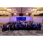
第4回 「デジタル・エンジニアリング・アワード」、世界の革新者とAI先駆者を称え、エンジニアリング・インテリジェンスの台頭を告げる
ボストン--(BUSINESS WIRE)--(ビジネスワイヤ) -- 「デジタル・エンジニアリング・アワード」は木曜日、米マサチューセッツ州ボストンで第4回を締めくくり、テクノロジー・ソリューションおよびAIの進歩への貢献をたたえて、技術分野の先駆者と組織を表彰しました。L&Tテクノロジー・サービシズ(BSE:540115、NSE:LTTS)が主催し、ISGが知見・調査パートナー、CNBC-TV18がメディアパートナーを務めたガラナイトには、北米、欧州をはじめ世界17か国から、業界リーダーと個人のチェンジメーカーが集いました。 主要企業・組織およびエンジニアリング分野の先駆者から寄せられた計258件の応募が、「エンジニアリング・ザ・チェンジ」(チーム)および「エンジニア・アット・ハート」(個人)の各部門で競い、12の異なる賞部門にまたがりました。Physical AI ImpactからDigital Engineering Project、Top Sustainability Initiative、Women Engineer of the Yearに至る各部門は、エンジニ...