Newsroom
Sorted by: Latest
-
Rapaport Press Release: Small-Diamond Recovery Accelerates in June
NEW YORK--(BUSINESS WIRE)--The recovery in prices for small diamonds gained momentum in June, with the 0.30- and 0.50-carat categories seeing sharper increases. The Rapaport Trade Diamond Index (RAPI™) rose 4.2% for 0.30-carat diamonds, up from a 2.1% gain in May. The 0.50-carat RAPI increased 1.3%, also higher than May’s 0.9% rise. The 1-carat index dipped 0.7%. RAPI for 3 carats rose 0.4%, turning positive after a May decline. Inventory reductions continued to support the upward price correct...
-
Concord Technologies Releases New Report on AI-Driven Interoperability and Operational Efficiency
SEATTLE--(BUSINESS WIRE)--Concord Releases Report on AI-Driven Interoperability and Operational Efficiency in American Hospital Association Market Scan Trailblazer report....
-
CaringAI Presents Research at AAIC 2026 Showing Strong Clinician Agreement with AI-Powered Telephone Cognitive Screening
RALEIGH, N.C.--(BUSINESS WIRE)--CaringAI, a healthcare technology company building an AI-powered voice agent platform for patient engagement, cognitive assessment, and dementia care, today announced research presented at the Alzheimer's Association International Conference (AAIC) 2026— the world's largest dementia research conference— in London. The study evaluates clinician agreement with CaringAI Listen, the company's telephone-based AI cognitive assessment platform, in real-world primary car...

-
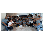
Riassunto: L'hackathon globale di EI di L&T Technology Services lancia la prossima ondata di soluzioni di ingegneria nativa AI
MONACO--(BUSINESS WIRE)--L&T Technology Services (BSE: 540115, NSE: LTTS), un leader globale nelle Soluzioni di Engineering Intelligence e nei servizi di consulenza ER&D, ha concluso con successo Engineering Intelligence (EI) OpenHack 2026, una sfida dell'innovazione globale prima nel suo genere, condotta simultaneamente in nove sedi ubicate in India, negli Stati Uniti e in Europa. L'hackathon ha riunito quasi 4.000 ingegneri (oltre 770 team) da Bengaluru, Mysuru, Chennai, Hyderabad, Pu...
-
Resumen: L&T Technology Services Global EI Hackathon despierta la próxima ola de soluciones de ingeniería nativas de IA
MÚNICH--(BUSINESS WIRE)--L&T Technology Services (BSE: 540115, NSE: LTTS),, líder internacional en soluciones de inteligencia de ingeniería y servicios de consultoría en ER&D, ha concluido con éxito el Engineering Intelligence (EI) OpenHack 2026, un desafío de innovación internacional único en su categoría que se ha celebrado simultáneamente en nueve sedes repartidas entre la India, Estados Unidos y Europa. El hackatón reunió a casi 4000 ingenieros (más de 770 equipos) de Bengaluru, Mys...

-
Globaler EI-Hackathon von L&T Technology Services stößt die nächste Welle KI-nativer Engineering-Lösungen an
MÜNCHEN--(BUSINESS WIRE)--L&T Technology Services (BSE: 540115, NSE: LTTS), ein weltweit führender Anbieter von Beratungsdienstleistungen in den Bereichen Engineering Intelligence Solutions & ER&D, hat Engineering Intelligence (EI) OpenHack 2026, den ersten globalen Innovationswettbewerb dieser Art, der gleichzeitig an neun Standorten in Indien, den USA und Europa stattfand, erfolgreich abgeschlossen. Der Hackathon brachte nahezu 4.000 Ingenieure (mehr als 770 Teams) aus Bengaluru,...

-
Le hackathon mondial d'ingénierie en intelligence artificielle de L&T Technology Services déclenche une nouvelle génération de solutions d'ingénierie IA natives
MUNICH--(BUSINESS WIRE)--L&T Technology Services (BSE : 540115, NSE : LTTS), un chef de file mondial des solutions d'intelligence d'ingénierie et des services de conseil en ER&D, a conclu avec succès le « Engineering Intelligence (EI) OpenHack 2026 », un défi d'innovation mondial inédit mené simultanément sur neuf sites répartis entre l'Inde, les États-Unis et l'Europe. Le hackathon a rassemblé près de 4 000 ingénieurs (plus de 770 équipes) provenant de Bengaluru, Mysuru, Chennai, Hyder...

-
Samenvatting: Wereldwijde EI-hackathon van L&T Technology Services ontketent de volgende golf engineeringoplossingen gebaseerd op AI
MÜNCHEN--(BUSINESS WIRE)--L&T Technology Services (BSE: 540115, NSE: LTTS), een wereldleider in Engineering Intelligence Solutions & ER&D Consulting Services, heeft met succes Engineering Intelligence (EI) OpenHack 2026 afgerond, een unieke internationale uitdaging die simultaan op negen plaatsen in India, de V.S. en Europa plaatsvond. De hackathon bracht om en bij 4.000 ingenieurs (meer dan 770 teams) uit Bengaluru, Mysuru, Chennai, Hyderabad, Pune, Vadodara, Mumbai, Dallas en Münc...

-
Digital Extremes Reveals the Future of Warframe and Soulframe Alongside Millions of Players at Annual TennoCon Celebration
LONDON, Ontario--(BUSINESS WIRE)--Digital Extremes celebrated 11 years of TennoCon with its record-breaking community celebration today attended by thousands of guests and streamed live to millions of fans around the world. Join more than 85 million other players and embark on the road ahead for Warframe, starting with the full gameplay reveal for Warframe: Tau, the next Narrative Chapter that takes players to an all-new Star Chart, the Tau System, launching for free on all platforms this year....

-
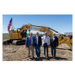
Janicki Industries Breaks Ground on $800 Million Campus in Great Falls Montana
GREAT FALLS, Mont.--(BUSINESS WIRE)--Janicki Industries, a privately owned engineering and manufacturing company, broke ground yesterday on its new manufacturing campus in Great Falls, Montana, marking the official start of construction on the company's $800 million investment in the region. The 1.6 million-square-foot campus, to be built in phases over the next decade, is expected to create 1,000 new jobs within five years and more than 2,000 jobs by the time it is complete. The groundbreaking...