

Newsroom
Sorted by: Latest
-
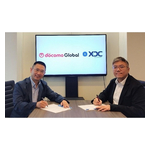
XDC Network Welcomes NTT DOCOMO GLOBAL as Institutional Masternode Validator
TOKYO--(BUSINESS WIRE)--XDC Network has deepened its roots in Japan, partnering with NTT DOCOMO GLOBAL, part of NTT DOCOMO Group, as an institutional masternode validator....
-
ReliaQuest and OpenAI Announce Partnership to Accelerate Agentic Cyber Defense for the Enterprise
TAMPA, Fla.--(BUSINESS WIRE)--ReliaQuest, the global leader in Agentic AI cybersecurity, today announced it is joining the OpenAI Daybreak Cyber Partner Program to accelerate the development and deployment of advanced AI capabilities for enterprise cyber defense. The program will provide ReliaQuest with closer technical collaboration and access to OpenAI’s frontier cyber capabilities and models to help enterprises find and patch vulnerabilities faster, while enabling security teams to keep pace...
-
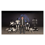
Faraday Future Founder and Global CEO YT Jia Shares Weekly Investor Update: Provides New Details on FF’s EAI Data Factory, Q3 “Four-Core Full-Stack AI” Robotics Practical Deployment Campaign and EAI Robotics Summer Camp
LOS ANGELES--(BUSINESS WIRE)--Faraday Future Intelligent Electric Inc. (NASDAQ: FFAI) (“Faraday Future”, “FF” or the “Company”), a California-based global Embodied AI (EAI) ecosystem company, today shared a weekly business update from YT Jia, Founder and Global CEO of FF.“Hello from issue 64 of our weekly report. Today, the FIFA World Cup Final has just concluded. Congratulations to Spain on lifting the World Cup, and congratulations to Lamine Yamal on reaching the biggest stage as one of the de...
-
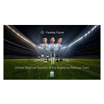
Faraday Future Announces Official Regional Sponsorship of the Argentina National Team in North America for Robotics and Related Technology, Bringing Together Physical AI Ecosystem and Global Soccer
LOS ANGELES--(BUSINESS WIRE)--Faraday Future Intelligent Electric Inc. (Nasdaq: FFAI) (“Faraday Future,” “FF,” or the “Company”), a U.S.-based Physical AI ecosystem company, today announced a partnership with the Argentine Football Association (“AFA”), under which FF will become an Official Regional Sponsor of the Argentina National Team in North America in the field of robotics and related robotics technology.The collaboration brings together two forces defined by continuous evolution and the p...
-
FIFA World Cup 2026™ Topps Final Halftime Show Makes History with Co-Headliners Justin Bieber, Madonna, Shakira and Burna Boy, BTS, the PS22 Chorus featuring Coldplay and Gustavo Dudamel
EAST RUTHERFORD, N.J.--(BUSINESS WIRE)--The first-ever FIFA World Cup™ Final Halftime Show made history today, bringing together a lineup of global superstars who captivated audiences around the world while advancing access to quality education for millions of children through the FIFA Global Citizen Education Fund. Produced by Global Citizen and curated by Chris Martin of Coldplay, the historic halftime show demonstrated the power of music to unite cultures and drive meaningful change, broadca...
-
HCA Investors Have Opportunity to Join HCA Healthcare, Inc. Fraud Investigation with the Schall Law Firm
LOS ANGELES--(BUSINESS WIRE)--HCA Investors Have Opportunity to Join HCA Healthcare, Inc. Fraud Investigation with the Schall Law Firm...
-
GPGI, Inc. Sued for Securities Law Violations - Contact the DJS Law Group to Discuss Your Rights – GPGI
LOS ANGELES--(BUSINESS WIRE)--GPGI, Inc. Sued for Securities Law Violations - Contact the DJS Law Group to Discuss Your Rights – GPGI...
-
ERIC Investors Have Opportunity to Join Telefonaktiebolaget LM Ericsson Fraud Investigation with the Schall Law Firm
LOS ANGELES--(BUSINESS WIRE)--ERIC Investors Have Opportunity to Join Telefonaktiebolaget LM Ericsson Fraud Investigation with the Schall Law Firm...
-
RXT Investors Have Opportunity to Join Rackspace Technology, Inc. Fraud Investigation with the Schall Law Firm
LOS ANGELES--(BUSINESS WIRE)--RXT Investors Have Opportunity to Join Rackspace Technology, Inc. Fraud Investigation with the Schall Law Firm...
-
UP Investors Have Opportunity to Join Wheels Up Experience Inc. Fraud Investigation with the Schall Law Firm
LOS ANGELES--(BUSINESS WIRE)--UP Investors Have Opportunity to Join Wheels Up Experience Inc. Fraud Investigation with the Schall Law Firm...