
 and CyberSpectrum Software. (Photo: Business Wire)")
 (Photo: Business Wire)")
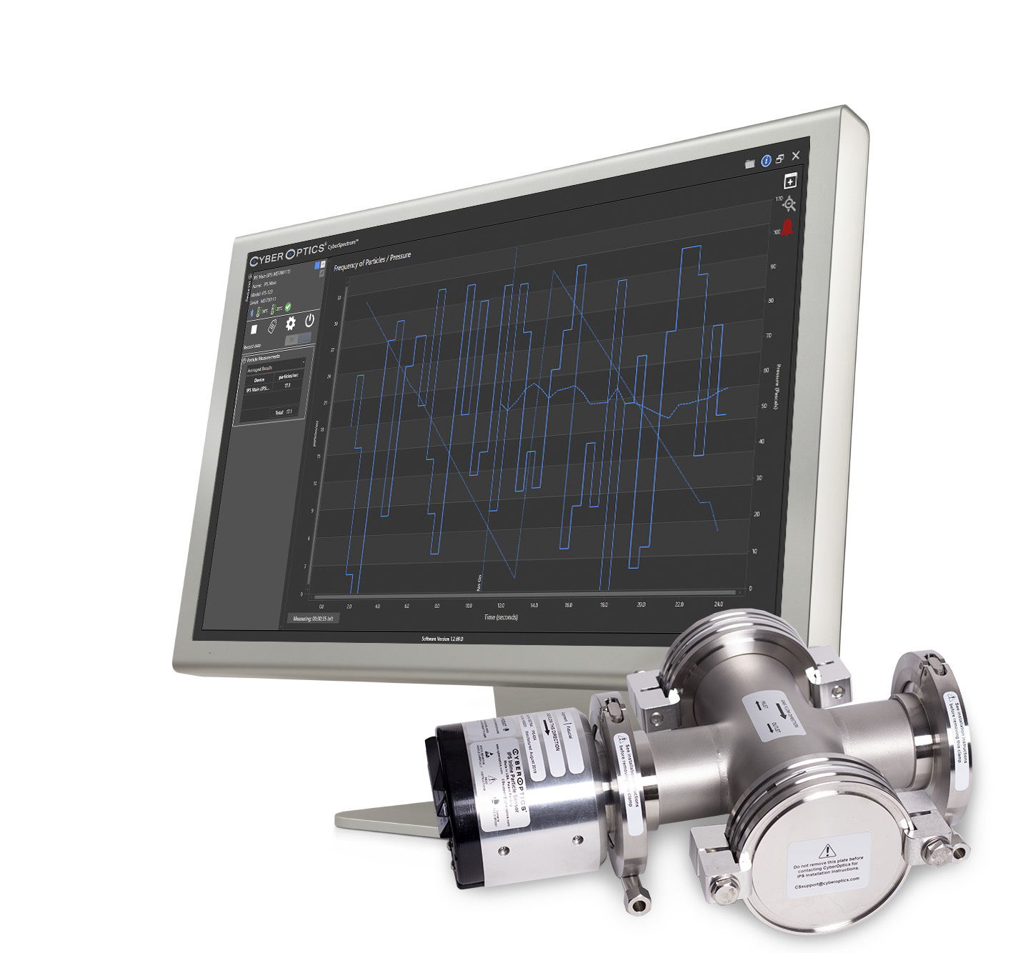
MINNEAPOLIS--(BUSINESS WIRE)--CyberOptics® Corporation (NASDAQ: CYBE), a leading global developer and manufacturer of high-precision 3D sensing technology solutions, will exhibit at SPIE Advanced Lithography from February 25-26, 2020 at the San Jose Convention Center in California, booth #308. During the show, the company will introduce its new In-Line Particle Sensor (IPS) with CyberSpectrum™ software for semiconductor tool set-up and equipment diagnostics.
An extension of the industry-leading WaferSense® and ReticleSense® Airborne Particle Sensor (APS) technology that is documented by fabs as the Best Known Method (BKM), the new In-Line Particle Sensor (IPS) with CyberSpectrum software detects particles in gas and vacuum lines 24/7 in semiconductor process equipment. The IPS quickly identifies, monitors and enables troubleshooting of particles down to 0.1µm.
The IPS can be installed in any gas or vacuum system, and is particularly relevant for EUVL tools where the ability to monitor particles in-line can significantly improve EUVL tool yield and productivity. For example, it can be installed at the vacuum line in between the EUV process chamber and the vacuum pump, saving significant time compared to current methods of sending a monitor dummy reticle into the system to check for particles before and after sending the reticle into the EUVL. The IPS is always on and collecting particle data, which is especially critical during chamber purging.
“We have incorporated our proprietary airborne particle sensing technology into an in-line form factor,” said Dr. Subodh Kulkarni, President and CEO, CyberOptics, “The IPS delivers the same benefits fabs worldwide have recognized with this proven technology. It can significantly save time and expense while improving yields and productivity.”
Process and equipment engineers in semiconductor fabs can speed equipment qualification with real-time, 24-7 monitoring, compare past and present data, as well as one tool to another. Contamination sources can be identified quickly and the effects of cleaning, adjustments and repairs can be seen in real-time. Fabs can shorten equipment maintenance cycles, lower equipment expenses and optimize preventative maintenance plans.
CyberOptics will also demonstrate the ReticleSense Airborne Particle Sensor (APSRQ) and the ReticleSense Auto Multi Sensor (AMSR) for wireless leveling, vibration, and relative humidity (RH) measurements.
For more information, visit www.cyberoptics.com.
About CyberOptics
CyberOptics Corporation (www.cyberoptics.com) is a leading global developer and manufacturer of high-precision 3D sensing technology solutions. CyberOptics’ sensors are used for inspection and metrology in the SMT and semiconductor capital equipment markets to significantly improve yields and productivity. By leveraging its leading edge technologies, the Company has strategically established itself as a global leader in high precision 3D sensors, allowing CyberOptics to further increase its penetration of key vertical markets. Headquartered in Minneapolis, Minnesota, CyberOptics conducts worldwide operations through its facilities in North America, Asia and Europe.
Statements regarding the Company’s anticipated performance are forward-looking and therefore involve risks and uncertainties, including but not limited to: market conditions in the global SMT and semiconductor capital equipment industries; trade relations between the United States and other countries; the timing of orders and shipments of our products, particularly our 3D MRS-enabled AOI systems; increasing price competition and price pressure on our product sales, particularly our SMT systems; the level of orders from our OEM customers; the availability of parts required to meet customer orders; unanticipated product development challenges; the effect of world events on our sales, the majority of which are from foreign customers; rapid changes in technology in the electronics and semiconductor markets; product introductions and pricing by our competitors; the success of our 3D technology initiatives; the market acceptance of our SQ3000 3D CMM system, products for semiconductor advanced packaging inspection and metrology and CyberGage360 product; costly and time consuming litigation with third parties related to intellectual property infringement; and other factors set forth in the Company’s filings with the Securities and Exchange Commission.