
")
SEOUL, South Korea--(BUSINESS WIRE)--Samsung Electronics Co., Ltd., a world leader in advanced semiconductor technology, today introduces its newest radio frequency (RF) technology based on 8-nanometer (nm) process.
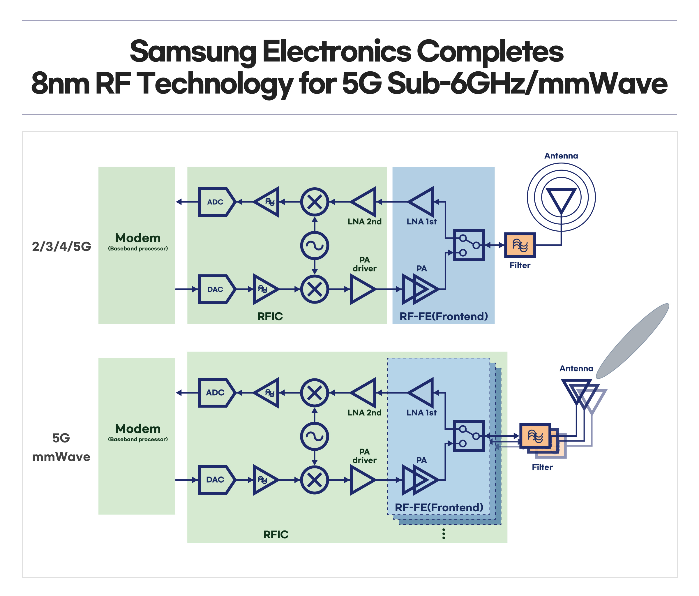
This cutting-edge foundry technology is expected to provide a “one chip solution,” specifically for 5G communications with support for multi-channel and multi-antenna chip designs. Samsung’s 8nm RF platform extension is expected to expand the company’s leadership in the 5G semiconductor market from sub-6GHz to mmWave applications.
Samsung’s 8nm RF process technology is the latest addition to an already broad portfolio of RF-related solutions, including 28nm- and 14nm-based RF. The company has established its RF market leadership through the shipping of more than 500 million mobile RF chips for premium smartphones since 2017.
“Through excellence in innovation and process manufacturing, we’ve reinforced our next-generation wireless communication offerings,” said Hyung Jin Lee, Master of Foundry Technology Development Team at Samsung Electronics. “As 5G mmWave expands, Samsung’s 8nm RF will be a great solution for customers looking for long battery life and excellent signal quality on compact mobile devices.”
Samsung’s New RFeFET™ Architecture
With continued scaling to advanced nodes, digital circuits have improved significantly in performance, power consumption, and area (PPA), whereas the analog/RF blocks haven’t enjoyed such an improvement due to degenerative parasitics such as increased resistance from narrow line width. As a result, most communications chips tend to see degraded RF characteristics such as deteriorated amplification performance of reception frequency and increased power consumption.
To overcome the analog/RF scaling challenges, Samsung has developed a unique architecture exclusive to 8nm RF named RFextremeFET (RFeFET™) that can significantly improve RF characteristics while using less power. In comparison to 14nm RF, Samsung’s RFeFET™ supplements the digital PPA scaling and restores the analog/RF scaling at the same time, thereby enabling high-performance 5G platforms.
Samsung’s process optimization maximizes channel mobility while minimizing parasitics. As the performance of RFeFET™ is greatly improved, the total number of transistors of RF chips and the area of analog/RF blocks can be reduced.
Compared to 14nm RF, Samsung’s 8nm RF process technology provides up to a 35-percent increase in power efficiency with a 35-percent decrease in the RF chip area as a result of the RFeFET™ architectural innovation.
About Samsung Electronics Co., Ltd.
Samsung inspires the world and shapes the future with transformative ideas and technologies. The company is redefining the worlds of TVs, smartphones, wearable devices, tablets, digital appliances, network systems, and memory, system LSI, foundry and LED solutions. For the latest news, please visit the Samsung Newsroom at news.samsung.com.