
")
SEOUL, South Korea--(BUSINESS WIRE)--Please replace the release with the following corrected version due to multiple revisions.
The corrected release reads:
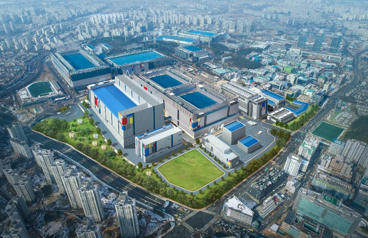
SAMSUNG ELECTRONICS BREAKS GROUND ON NEW EUV LINE IN HWASEONG
Construction will be completed in the second half of 2019 and ready for production in 2020
Samsung aims to maintain its leadership in cutting-edge process technology under 7nm
Samsung Electronics Co., Ltd., a world leader in advanced semiconductor technology, today announced that it broke ground on a new EUV (extreme ultraviolet) line in Hwaseong, Korea, aiming to maintain its leadership in state-of-the-art semiconductor technology.
With this new EUV line, Samsung will be able to strengthen its leadership in the single nanometer process technology by responding to market demand from various applications, including mobile, server, network, and HPC (high performance computing), for which high performance and power efficiency are critical.
The new facility is expected to be completed within the second half of 2019 and start production ramp-up in 2020. The initial investment in this new EUV line is projected to reach USD 6 billion by 2020 and additional investment will be determined depending on market circumstances.
"With the addition of this new EUV line, Hwaseong will become the center of the company's semiconductor cluster spanning Giheung, Hwaseong and Pyeongtaek," said Kinam Kim, President & CEO of Device Solutions at Samsung Electronics. "The line will play a pivotal role as Samsung seeks to maintain a competitive edge as an industry leader in the coming age of the Fourth Industrial Revolution."
Samsung has decided to utilize cutting-edge EUV technology starting with its 7-nanometer (nm) LPP (Low Power Plus) process. This new line will be set up with EUV lithography equipment to overcome nano-level technology limitations. Samsung has continued to invest in EUV R&D to support its global customers for developing next-generation chips based on this leading-edge technology.
About Samsung Electronics Co., Ltd.
Samsung inspires the world and shapes the future with transformative ideas and technologies. The company is redefining the worlds of TVs, smartphones, wearable devices, tablets, digital appliances, network systems, and memory, system LSI, foundry and LED solutions. For the latest news, please visit the Samsung Newsroom at http://news.samsung.com.